Semiconductor integrated circuit device and wireless communication device

a wireless communication and integrated circuit technology, applied in the direction of pulse automatic control, oscillator stabilization, generator, etc., can solve the problems of phase noise performance fluctuation phase noise performance deterioration by nois

Inactive Publication Date: 2006-07-13
KK TOSHIBA
View PDF4 Cites 13 Cited by
  • Summary
  • Abstract
  • Description
  • Claims
  • Application Information

AI Technical Summary

Benefits of technology

[0022] According to an aspect of the invention is to provide a semiconductor integrated circuit device comprising a voltage controlled oscillation circuit, a maximum value detection circuit to detect a maximum value of an oscillation output signal of the voltage controlled oscillation circuit, a minimum value detection circuit to detect a minimum value of the oscillation output signal of the voltage controlled oscillation circuit, a first reference voltage generation circuit to output a first predete

Problems solved by technology

In a conventional voltage controlled oscillation circuit, there is a problem that phase noise performance deteriorates by a noise when the amplitude of the oscillation output signal is too small.
There is also a problem that the phase noise performance deteriorates by a distortion of the oscillation output signal when the amplitude of the oscillation output signal is too large.
However, it causes a problem that the phase noise performance fluctuates because the amplitude of the oscillation output signal fluctuates b

Method used


Image

  • Semiconductor integrated circuit device and wireless communication device
  • Semiconductor integrated circuit device and wireless communication device
  • Semiconductor integrated circuit device and wireless communication device

Examples


first embodiment

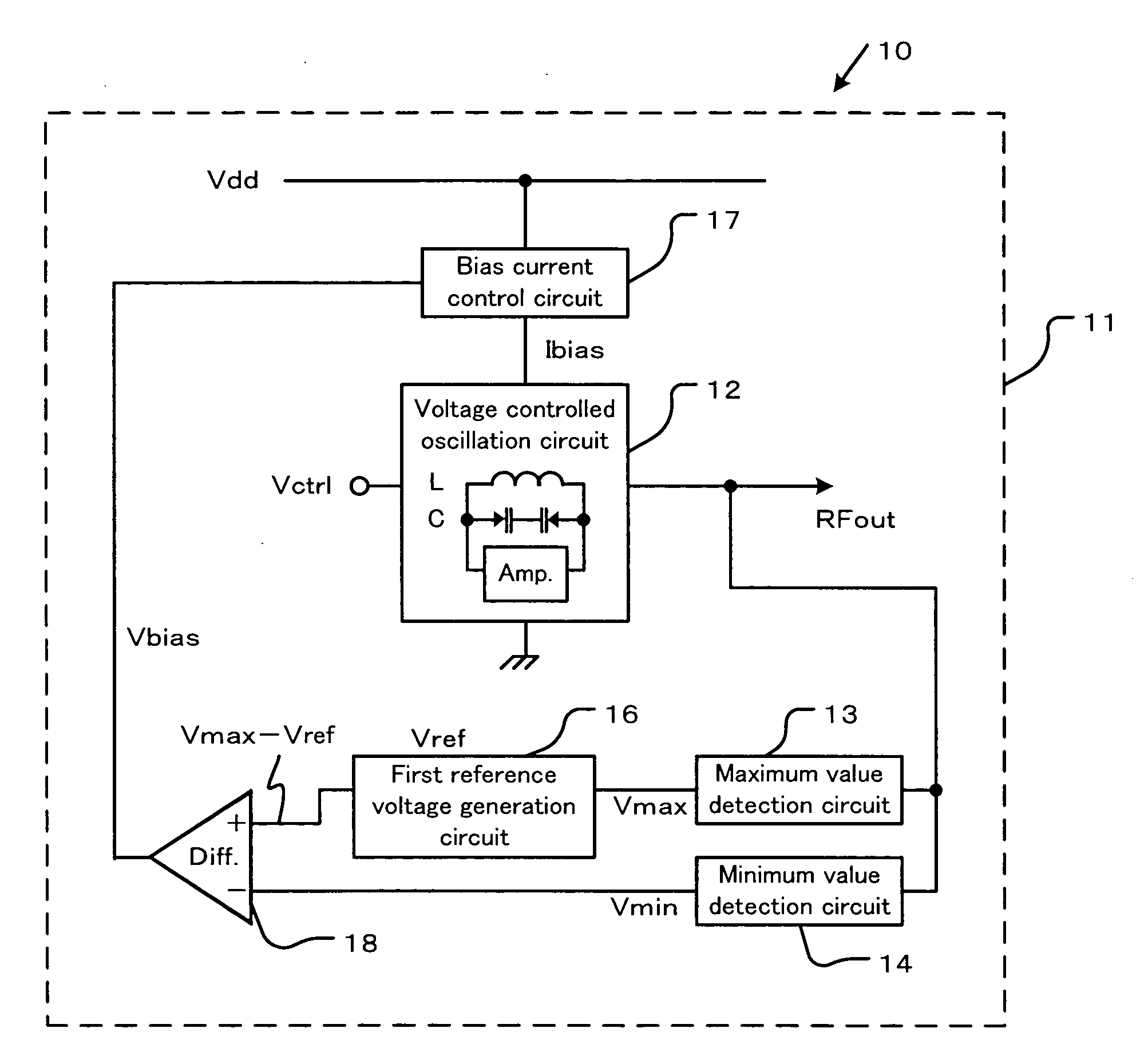
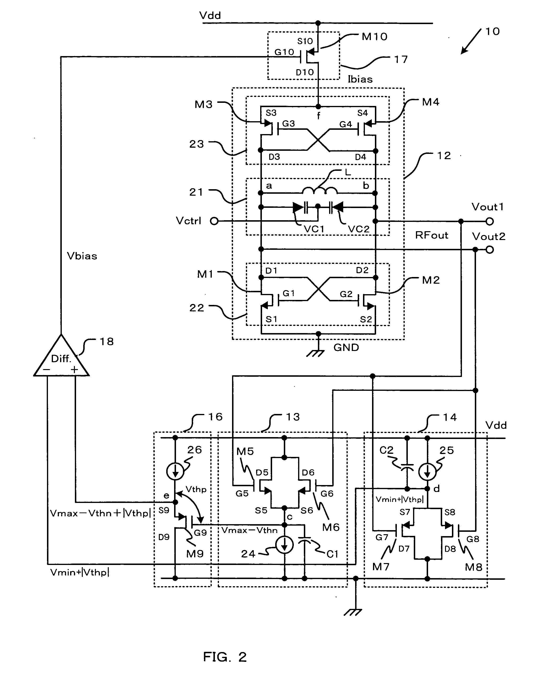
[0071] The solid line a shows a result of a simulation according to the The broken line b shows a result of a simulation according to a conventional circuit, where a voltage controlled oscillation circuit is not provided with the maximum value detection circuit 13, the minimum value detection circuit 14, the first reference voltage generation circuit 16, the bias current control circuit 17 and the differential amplifier 18.

[0072] In the first embodiment, the phase noise performance are constant approximately with −105 dBc / Hz at 200 kHz offset from a 4.8 GHz carrier and −135 dBc / Hz at 6 GHz offset from a 4.8 GHz carrier respectively even though the threshold voltage of the MOSFET changes. While in the conventional circuit, the phase noise performance drastically deteriorated by the threshold voltage deviation ±0.1V from the designed value as for the standard threshold voltage.

[0073] In the first embodiment, the bias current Ibias changes so that the difference between the maximum v...

second embodiment

[0098] In the second embodiment, it is possible that the phase noise performance is tuned because the difference between the maximum value and the minimum value of the oscillation output signal RFout is adjusted when the power supply voltage is initially provided or when it is needed.

[0099] As shown in FIG. 7A, the semiconductor integrated circuit device of the second embodiment is provided with a comparator 60 having two input terminals and output terminal, one of the input terminals is connected to the node e of the first reference voltage generation circuit 16, the other of the input terminals is connected to the node d of the minimum value detection circuit 14, a bias current sweep circuit 61 coupled between the comparator 60 and the bias current control circuit 17.

[0100] Synchronized with a clock signal CLK, the comparator 60 compares the voltage Vmax−Vthn+|Vthp| with the voltage Vmin+|Vthp|. The result of the comparison is provided to one of input terminals of a logical produ...

third embodiment

[0114] As shown in FIG. 8A, the semiconductor integrated circuit device of the third embodiment is provided with a bias current sweep circuit 71 and a bias current control circuit 73. The bias current sweep circuit 71 includes the AND circuit 62, the counter 63 and a decoder 70 to decode the count value of the counter 63. The decoded signal is provided to the bias current control circuit 73.

[0115] The bias current control circuit 73 includes a plurality of the switching transistors 72. A plurality of gates G72 of the switching transistors 72 is connected to a plurality of the output terminals of the decoder 70 respectively. A plurality of sources S72 of the switching transistors 72 is connected to the power supply voltage Vdd. A plurality of drains D72 of the switching transistors 72 is connected to the voltage controlled oscillation circuit 12.

[0116] The counter 63 is reset when the tuning signal TUNE is provided. The tuning signal TUNE is provided when the power supply voltage Vd...


PUM


Abstract

A semiconductor integrated circuit device having a voltage controlled oscillation circuit that is capable of sufficient oscillation performance and a wireless communication device having the semiconductor integrated circuit device are disclosed. A difference between the maximum value and the minimum value of the oscillation output signal is automatically controlled to be substantially equal to the first predetermined voltage which is the threshold voltage of the oscillation MOSFET for sufficient phase noise performance. It is further disclosed that the difference between the maximum value and the minimum value of the oscillation output signal may be varied by the change of the threshold voltage of the MOSFET caused by substrate bias effect, while maintaining the sufficient phase noise performance.

Description

CROSS REFERENCE TO RELATED APPLICATION [0001] This application is based upon and claims the benefit of priority from the prior Japanese Patent Application No. 2004-365787, filed on Dec. 17, 2004, the entire contents of which are incorporated herein by reference. FIELD OF THE INVENTION [0002] The present invention relates to a semiconductor integrated circuit device and a wireless communication device, which is capable of sufficient oscillation performance. DESCRIPTION OF THE BACKGROUND [0003] A wireless communication device such as a mobile phone which is provided with a voltage controlled oscillation circuit is widely used. The oscillation frequency of the voltage controlled oscillation circuit may be varied by a control voltage. [0004] In a conventional voltage controlled oscillation circuit, there is a problem that phase noise performance deteriorates by a noise when the amplitude of the oscillation output signal is too small. There is also a problem that the phase noise performa...

Claims


Application Information

Patent Timeline
IPC IPC(8): H03L7/099
CPCH03L5/00H03B5/1228H03B5/1215H03B5/1243
Inventor MIYASHITA, DAISUKEISHIKURO, HIROKI
Owner KK TOSHIBA
Why Eureka
Try Eureka