Low-power delay buffer circuit

a delay buffer and low-power technology, applied in the field of delay buffers, can solve the problems of mainly power consumption of sram-based delay buffers, limited capacity to sustain these devices, and high power consumption, and achieve the effect of less layout area

Active Publication Date: 2006-07-13
NAT TAIWAN UNIV
View PDF1 Cites 7 Cited by
  • Summary
  • Abstract
  • Description
  • Claims
  • Application Information

AI Technical Summary

Benefits of technology

[0007] The major objective of the present invention is to provide a low-power delay buffer circuit, which not only could achieve a power consumption eve

Problems solved by technology

Most of the mobile communications devices are powered by a battery and, as these devices are getting increasingly complicated and functional-rich, how to let batteries of a limited capacity to sustain these devices for the longest operation time concerns a

Method used


Image

  • Low-power delay buffer circuit
  • Low-power delay buffer circuit
  • Low-power delay buffer circuit

Examples


Embodiment Construction

[0024] In the following, detailed description along with the accompanied drawings is given to better explain preferred embodiments of the present invention.

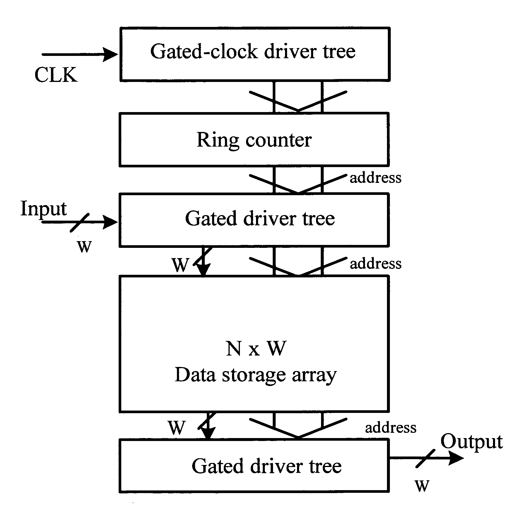
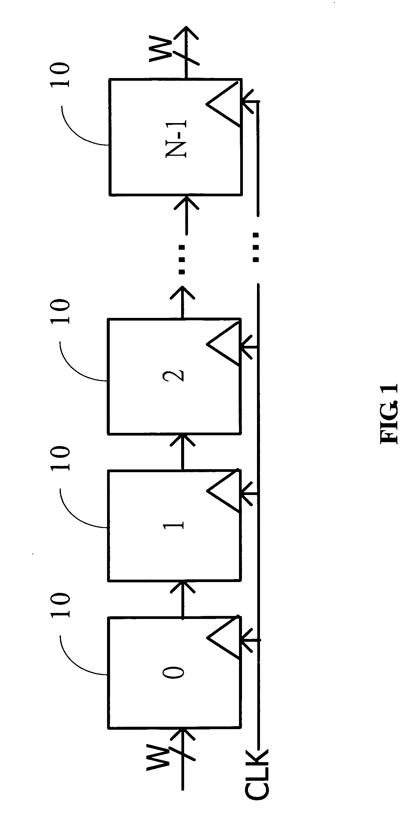
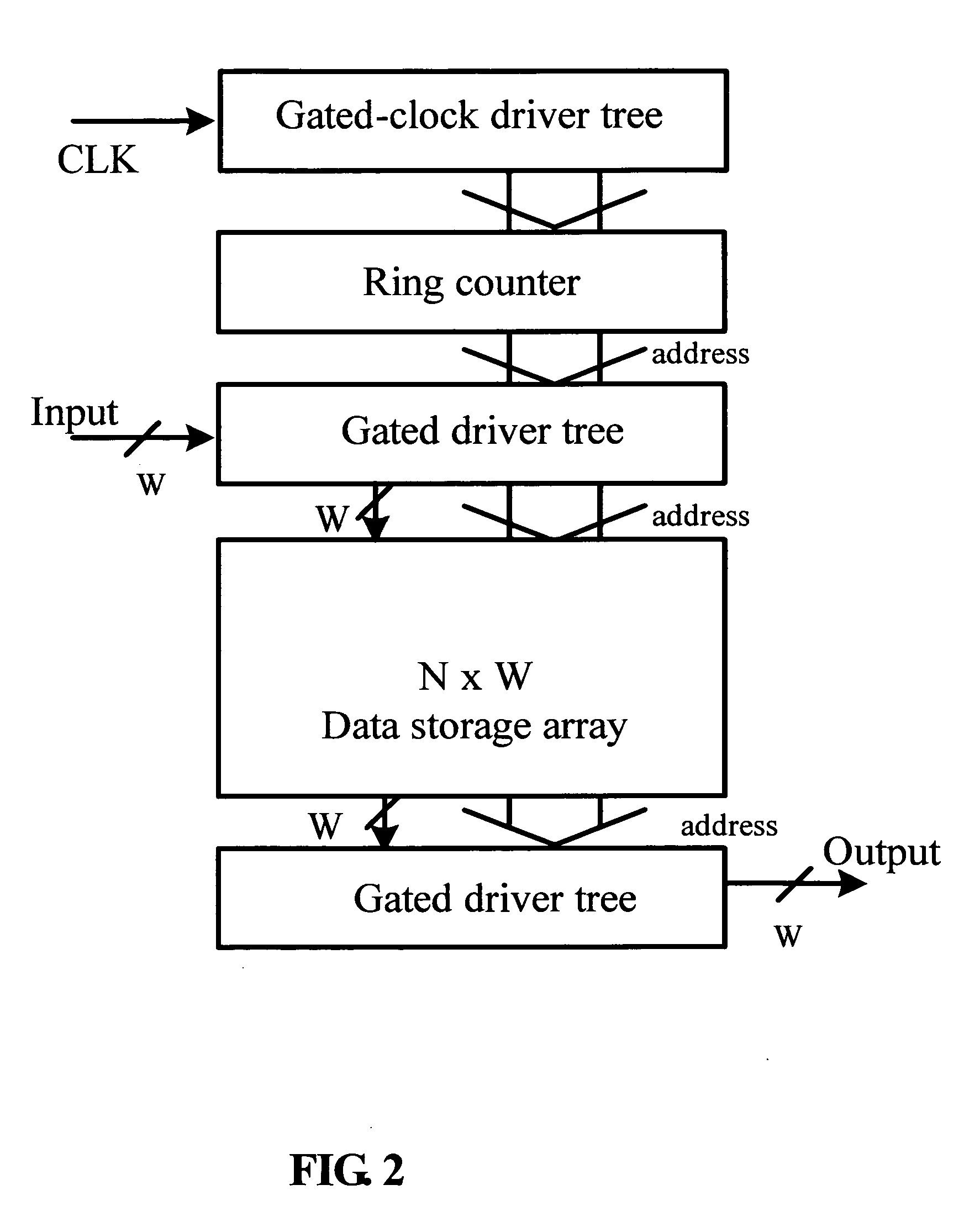
[0025] The delay buffer circuit of the present invention utilizes a ring counter as an address decoder similar to that of a SRAM memory. In addition, a latch array or similar memory is used for the storage of data. FIG. 3 is a schematic diagram showing an N×W delay buffer circuit composed of a ring counter and a latch array. As illustrated, the latch array is composed of N groups of latches 22 and each group of latches 22 contains W latches (not shown in FIG. 2), jointly for the storage a W-bit data. The input port D and output port Q of the N groups of latches 22 are connected to the input bus 21 and output bus 23, which in turn connect to two registers 24 and 25 respectively. The ring counter is composed of N series-connected shift registers 20, with the output of the last shift register 20 (numbered N−1) looped back to the in...


PUM


Abstract

A low-power delay buffer circuit is provided, which utilizes a ring counter as address decoder and a latch array for memory. To reduce power consumption, a gated-clock driver tree is applied to the ring-counter addressing architecture. Moreover, a similar gated-driver tree is applied to the input and output ports of the latch array. The delay buffer circuit not only could achieve a power consumption lower than SRAM-based delay buffers, but also could operation under high frequencies and take up less layout area than SRAM-based delay buffers.

Description

BACKGROUND OF THE INVENTION [0001] 1. Field of the Invention [0002] The present invention generally relates to delay buffers, and more particularly to a delay buffer circuit using gated driver tree architecture. [0003] 2. The Prior Arts [0004] In recent years, as wireless networks are gaining widespread popularity, numerous communications standards are established and adopted, mobile communications devices such as handsets, personal digital assistants (PDA), etc., have become the mainstream product of consumer electronics market. Most of the mobile communications devices are powered by a battery and, as these devices are getting increasingly complicated and functional-rich, how to let batteries of a limited capacity to sustain these devices for the longest operation time concerns all product vendors. One of the approaches is of course to reduce the power consumption of these devices' relevant circuits. [0005] In a digital processing chip of mobile communications, the delay buffer ta...

Claims


Application Information

Patent Timeline
IPC IPC(8): G11C7/00G06F5/10G11C7/22G11C8/04G11C8/18G11C19/00H03L7/06
CPCG06F5/10G06F2205/104G11C7/22G11C8/04G11C8/18G11C19/00
Inventor CHIUEH, TZI-DARHSIEH, PO-CHUN
Owner NAT TAIWAN UNIV
Why Eureka
Try Eureka