

Semiconductor device having dual gate electrode and related method of formation
- Summary
- Abstract
- Description
- Claims
- Application Information
AI Technical Summary
Benefits of technology
Problems solved by technology
Method used
Image

Examples
Embodiment Construction
[0016] Reference will now be made in some additional detail to exemplary embodiments of the invention, examples of which are illustrated in the accompanying drawings. However, the invention is not limited to only the embodiments described herein.
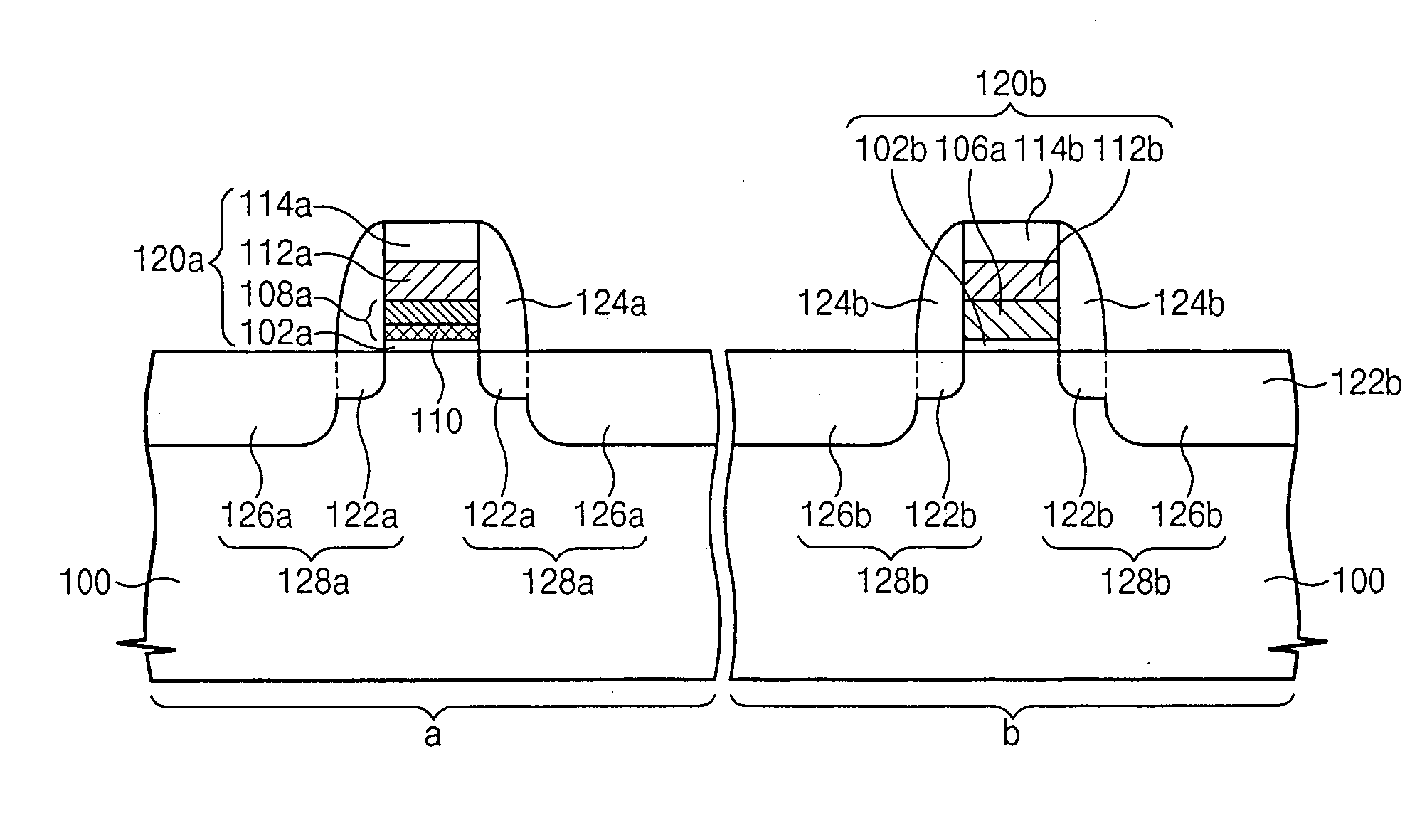
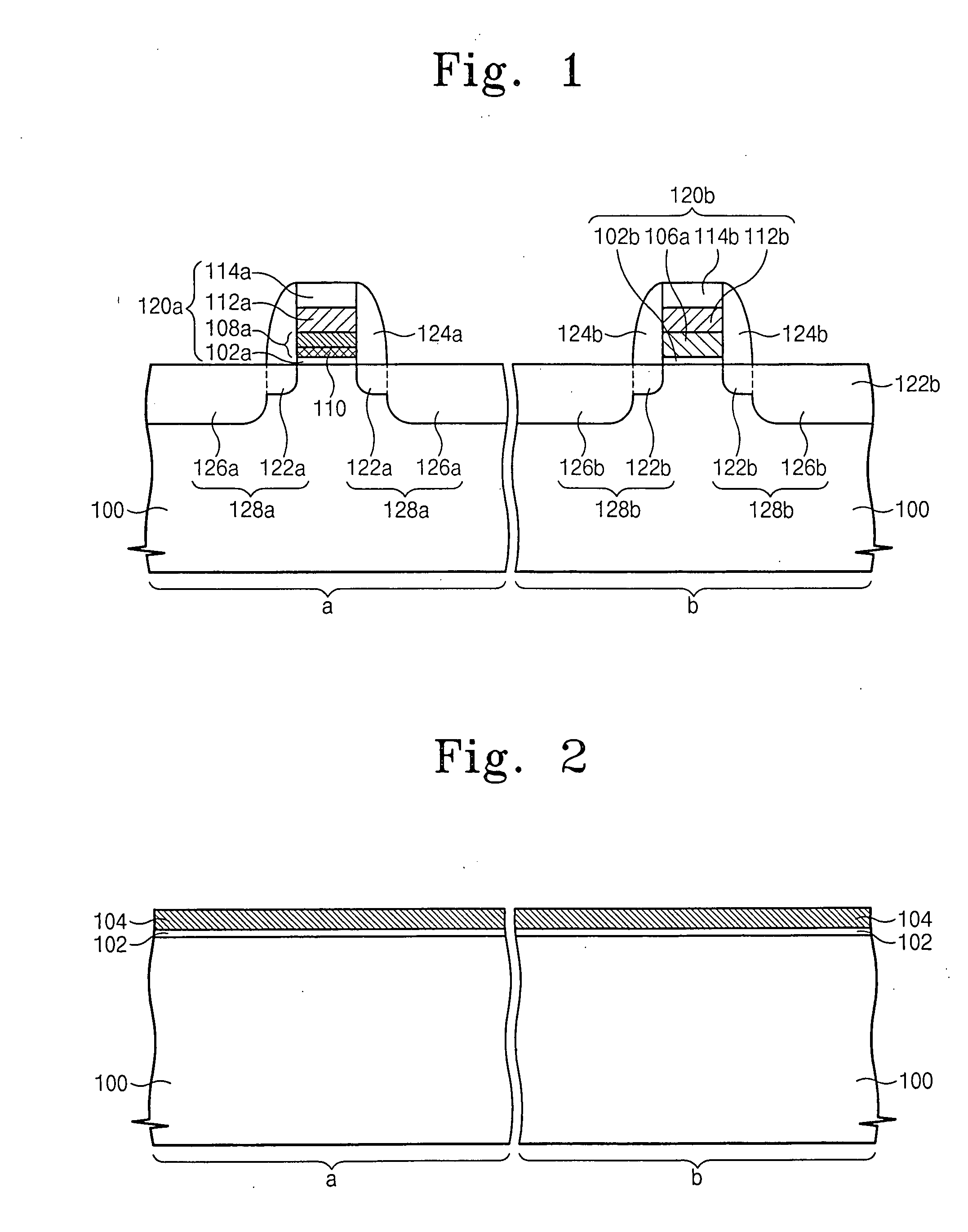
[0017]FIG. 1 is a cross-sectional view of a semiconductor device having a dual gate electrode according to one embodiment of the invention.
[0018] Referring to FIG. 1, a semiconductor substrate 100 comprises a first region “a” and a second region “b”. One of the first region “a” and the second region “b” is an NMOS region where an NMOS transistor is formed and the other is a PMOS region where a PMOS transistor is formed.
[0019] A first gate pattern 120a is formed on the first region of semiconductor substrate 100, and a second gate pattern 120b is formed on the second region of semiconductor substrate 100. A device isolation layer (not shown) may also be formed in a predetermined region of semiconductor substrate 100 to define a first activ...
PUM
 Abstract
Description
Claims
Application Information