Electrooptic device, method for producing the same, and electronic apparatus

a technology of electrooptic devices and electronic devices, applied in the direction of discharge tubes/lamp details, organic semiconductor devices, discharge tubes/lamp details, etc., can solve the problems of easy uneven brightness in the image display region, affecting the operation properties of electrooptic devices, and reducing the optical variation in the electrooptic conversion region. , the effect of reducing the optical variation in the electrooptic conversion region

Active Publication Date: 2006-07-20
ELEMENT CAPITAL COMMERCIAL CO PTE LTD
View PDF16 Cites 107 Cited by
  • Summary
  • Abstract
  • Description
  • Claims
  • Application Information

AI Technical Summary

Benefits of technology

[0009] An advantage of the present invention is that it provides an electrooptic device that has reduced optical variation in electrooptic conversion regions, achieves high reliability, and realizes high-quality conversion; and a method for making the electrooptic device. Various electronic apparatuses incorporating such electrooptic devices are also provided.
[0010] A first embodiment of the invention provides an electrooptic device that includes a first substrate and a second substrate. The first substrate includes an electrooptic element in which an electrooptic substance is interposed between a first electrode and a second electrode, the electrooptic element being disposed on a surface of the first substrate that opposes the second substrate; an electronic element for driving the electrooptic element; and a power supply wire for supplying power to at least one of the electrooptic element and the electronic element. The second substrate includes a second auxiliary wire for supplying auxiliary power to at least one of the electrooptic element and the electronic element, the second auxiliary wire being disposed on a surface of the second substrate that opposes the first substrate, the second auxiliary wire having a planar shape that corresponds with a non-opening region of the electrooptic element.
[0011] With this structure, power is supplied to at least one of the electrooptic element and the electronic element through the poser supply wire during operation. This induces electrooptic operation in the electrooptic element including the electrooptic substance sandwiched between the electrodes. Here, auxiliary power is supplied to the second auxiliary wire having a low resistance. Thus, although the resistance of the power supply wire is high, it becomes possible to reduce the voltage drop caused by the power supply wire. For the purpose of this specification, the term “electrooptic substance” refers to a substance that converts electrical signals to light and vice versa. One example thereof is an organic light-emitting substance. The term “electronic element” refers to, for example, an active element such as a thin film transistor (TFT) and may include passive elements, such as storage capacitors. In an organic EL device of an active matrix type, one organic EL element is provided for each unit circuit, and is driven and controlled by the circuit.
[0012] In this invention, some of the components that have been formed on the first substrate are moved onto the second substrate, and the first substrate and second substrate are made in separate processes. For example, by forming auxiliary wires of the power supply wire on the second substrate, it becomes possible to form auxiliary wires having a complicated shape and low resistance without being affected by the characteristics of environment-sensitive organic EL elements and other peripheral elements or the limitations derived from the laminated structure. Moreover, such an arrangement does not affect the characteristics of the organic EL elements and the peripheral elements.
[0013] As a result, variation in brightness due to power supply cross talk can be reduced, and large-screen, high-quality image display devices can be provided.
[0014] According to an embodiment of the electrooptic device, the second electrode is closer to the second substrate than the first electrode is; a spacer for regulating the distance between the first substrate and the second substrate is disposed on the first substrate or the second substrate such that the spacer is adjacent to the electrooptic element; and a connecting portion for supplying power from the second auxiliary wire to the second electrode is disposed on a surface of the spacer.

Problems solved by technology

Even when these electrodes and power supply wires are composed of low-resistance metal materials, the resistance of the electrode and power supply wire causes the power voltage to decrease with the increase in size and output (brightness) of the electrooptic devices.
This also affects the operation properties of the electrooptic devices.
As a result, unevenness in brightness in the image display region readily occurs.
Consequently, in attempting to apply the device to a thin-film light-emitting device of an active drive type, such as an organic EL display device, by increasing the size, the thickness of the wiring (power supply wire) cannot be simply increased.
Thus, the display quality is significantly degraded, and increasing the size, the resolution, and / or the brightness of the device is difficult.
However, the above-described related techniques have a limit in reducing the resistance due to the power supply wire.
Moreover, due to the limitations derived from planarizing technology for laminating active drive elements and organic EL elements and damages inflicted therefrom, reduction of electrode resistance has been complicated and difficult.
Moreover, the provided solution did not satisfy conflicting requirements, such as brightness and driving current, required for electrooptic devices.
This significantly reduces the reliability of the electrooptic device.
Since a larger stress is applied onto the region overlapping the spacer, short-circuiting of the conductive film or microcracks or breaking of the insulating film easily occur when the conductive film pattern is deformed.

Method used


Image

  • Electrooptic device, method for producing the same, and electronic apparatus
  • Electrooptic device, method for producing the same, and electronic apparatus
  • Electrooptic device, method for producing the same, and electronic apparatus

Examples


first embodiment

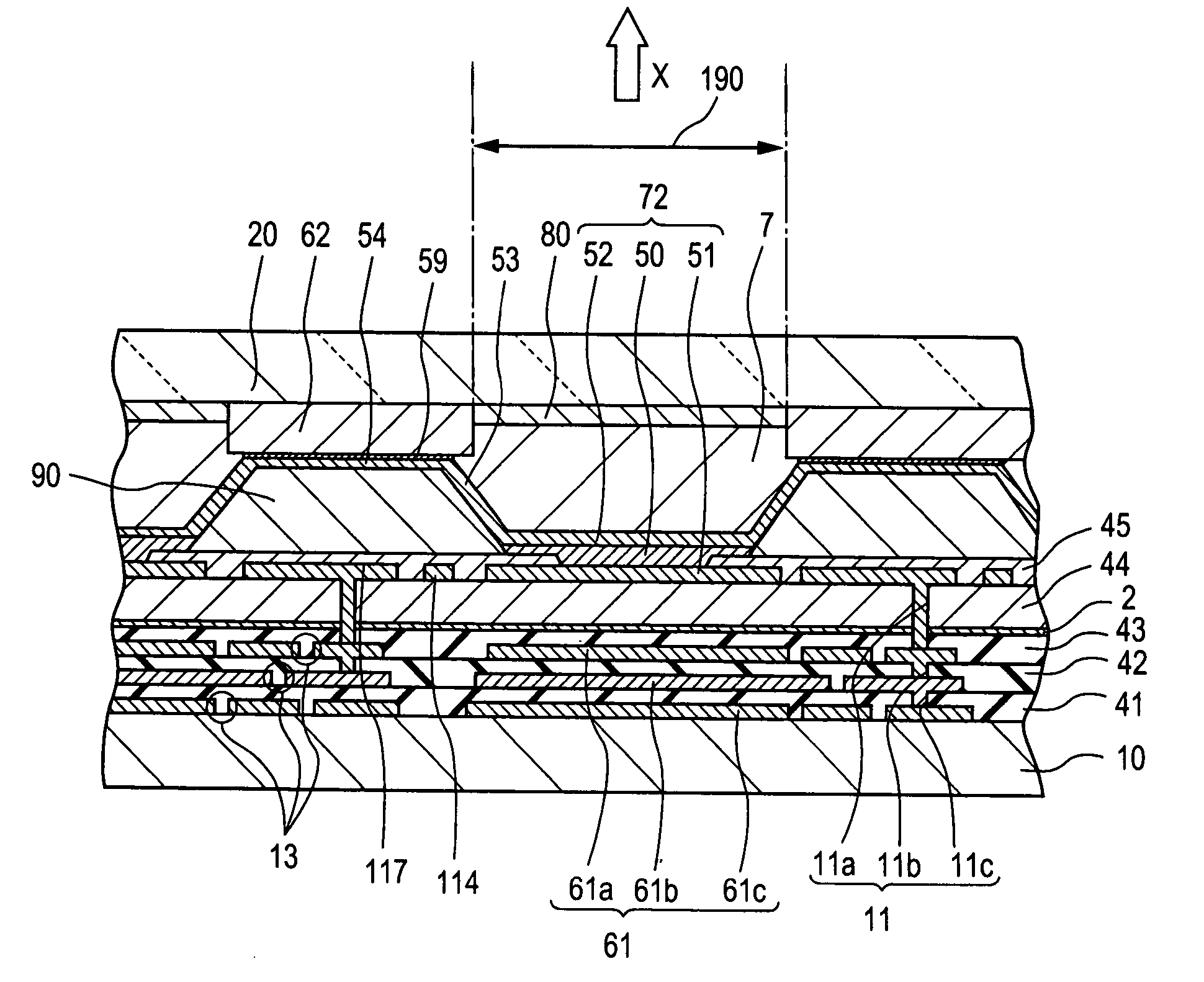
[0095] The overall structure of the organic EL device of a first embodiment and the structure of the pixel unit are first described with reference to FIGS. 1 to 10.

Overall Structure of Organic EL Device

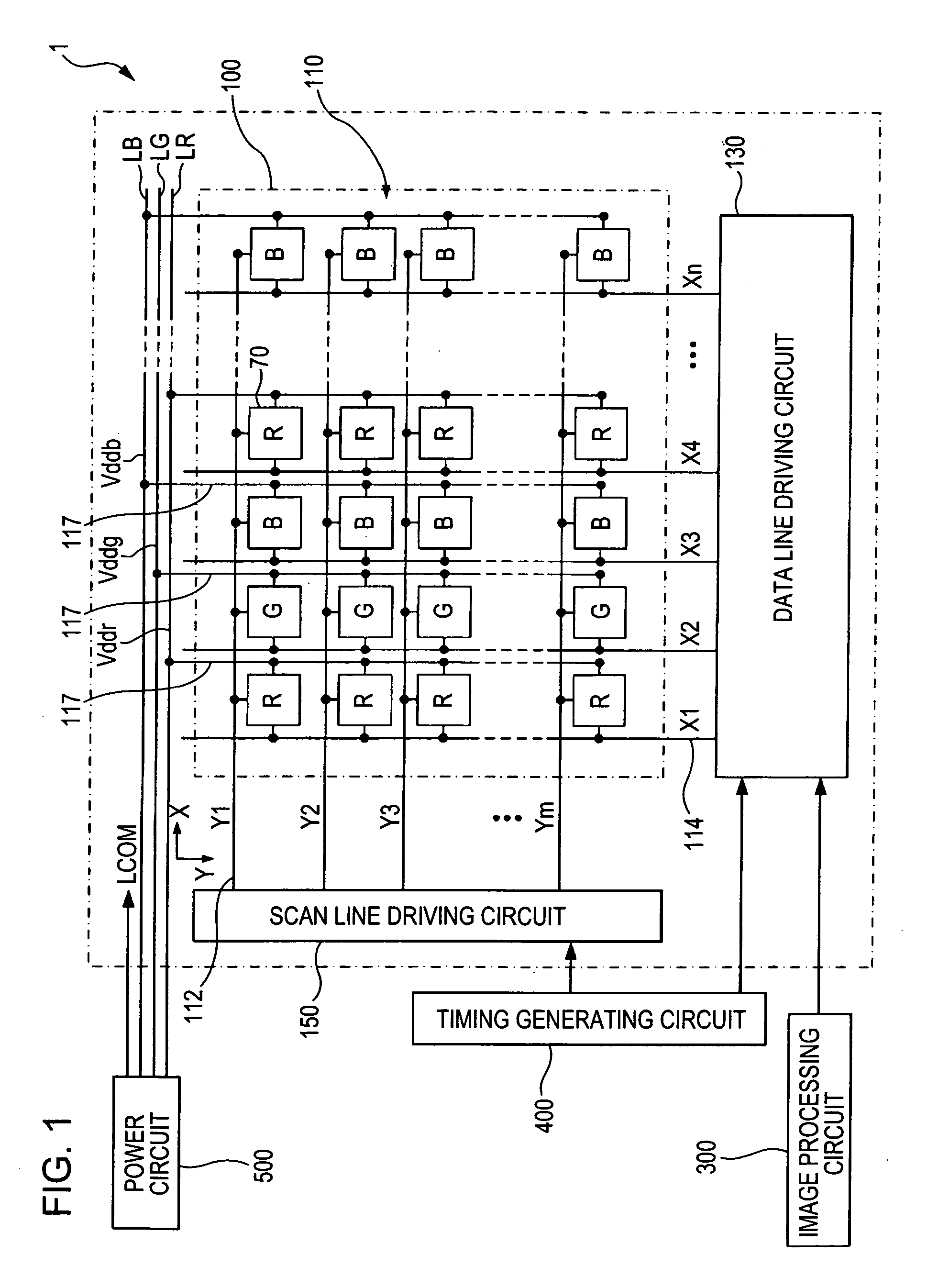
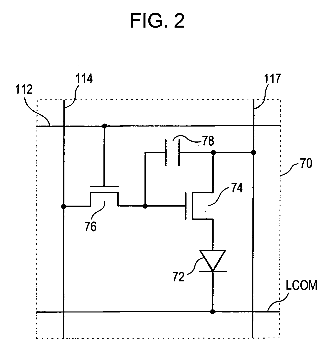
[0096]FIG. 1 is a block diagram showing the overall structure of the organic-EL device of this embodiment. FIG. 2 is a circuit diagram showing the structure of a particular pixel unit.

[0097] In FIG. 1, an organic EL device 1, which is an example of the electrooptic device, has an organic EL panel 100, a power circuit 500, a scan line driving circuit 150, a data line driving circuit 130, an image processing circuit 300, and a timing generating circuit 400 as the main components.

[0098] The organic EL panel 100 has the number m (wherein m is a natural number of 2 or more) of scan lines 112 arranged in parallel to the X direction and the number n (wherein n is a natural number of 2 or more) of data lines 114 arranged in parallel to the Y direction orthogonal to the X direction. The s...

second embodiment

[0172] An organic EL device according to a second embodiment will now be described with reference to FIG. 11. FIG. 11 is a cross-sectional view similar to that of the first embodiment shown in FIG. 4. In FIG. 11, the components identical with those of the first embodiment shown in FIG. 4 are represented by the same reference numerals and the descriptions therefor are omitted.

[0173] As shown in FIG. 11, the light-scattering layer 80 of the second embodiment has a shape of a lens. Thus, the light generated in the organic EL element 72 can be focused through the light-scattering layer 80 in a perpendicular direction with respect to the second substrate. Thus, the light-extraction efficiency can be further increased. The lens-shaped light-scattering layer 80 is interposed between the first substrate 10 and the second substrate 20 so that the light extraction efficiency can be further increased compared to when the light-scattering layer 80 is provided outside the second substrate 20. T...

third embodiment

[0177] An organic EL device according to a third embodiment will now be described with reference to FIGS. 12 and 13. FIG. 12 is a plan view showing a second auxiliary wire of the third embodiment. FIG. 13 is a cross-sectional view of a pixel unit of the third embodiment taken along line XIII-XIII in FIG. 12. In FIGS. 12 and 13, the components similar to those of the first embodiment shown in FIGS. 1 to 10 are represented by the same reference numerals, and the descriptions therefor are omitted.

[0178] As shown in FIG. 12, the organic EL device of the third embodiment has a fine second auxiliary wire 62 has fine lines 164 in the opening region 190 of the organic EL element 72.

[0179] The second auxiliary wire 62 contains a low-reflection material and has a particular planar pattern that at least partly covers the non-opening region of the pixel unit 70. In this manner, the second auxiliary wire 62 also serves as a black mask or a black matrix. In addition, as shown in FIGS. 12 and 13...


PUM


Abstract

An electrooptic device includes a first substrate and a second substrate. The first substrate includes an electrooptic element in which an electrooptic substance is interposed between a first electrode and a second electrode, the electrooptic element being disposed on a surface of the first substrate that opposes the second substrate; an electronic element for driving the electrooptic element; and a power supply wire for supplying power to at least one of the electrooptic element and the electronic element. The second substrate includes a second auxiliary wire for supplying auxiliary power to at least one of the electrooptic element and the electronic element, the second auxiliary wire being disposed on a surface of the second substrate that opposes the first substrate, the second auxiliary wire having a planar shape that corresponds with a non-opening region of the electrooptic element.

Description

BACKGROUND [0001] 1. Technical Field [0002] The present invention relates to the technical fields of electrooptic devices, such as organic electroluminescent (EL) devices, production methods therefor, and various electronic apparatuses including the electrooptic devices. [0003] 2. Related Art [0004] In electrooptic devices, such as organic EL devices and silicon light-emitting devices, that include solid thin films and are driven and controlled by active elements such as TFTs, the electrodes and power supply wires of the electrooptic devices are composed of thin films. Even when these electrodes and power supply wires are composed of low-resistance metal materials, the resistance of the electrode and power supply wire causes the power voltage to decrease with the increase in size and output (brightness) of the electrooptic devices. This also affects the operation properties of the electrooptic devices. When the electrooptic devices is a display device of an active drive type in whic...

Claims


Application Information

Patent Timeline
Patent Type & Authority Applications(United States)
IPC IPC(8): H05B33/08H05B33/06H05B44/00
CPCH01L27/3211H01L27/3244H01L27/3279H01L51/0024H01L51/5212H01L51/5228H01L51/525H01L51/5268H01L51/5271H01L51/5275H01L51/5284H01L51/529H01L51/56H01L2251/5315H10K59/35H10K59/122H10K59/12H10K59/1315H10K71/50H10K50/814H10K50/824H10K50/8428H10K50/854H10K50/858H10K50/856H10K50/87H10K50/865H10K71/00H10K2102/3026H05B33/26H05B33/10
Inventor IMAMURA, YOICHI
Owner ELEMENT CAPITAL COMMERCIAL CO PTE LTD
Why Eureka
Try Eureka