
Optical transmission and/or receiving device

Inactive Publication Date: 2006-07-27
II VI DELAWARE INC
View PDF4 Cites 2 Cited by
  • Summary
  • Abstract
  • Description
  • Claims
  • Application Information

AI Technical Summary

Benefits of technology

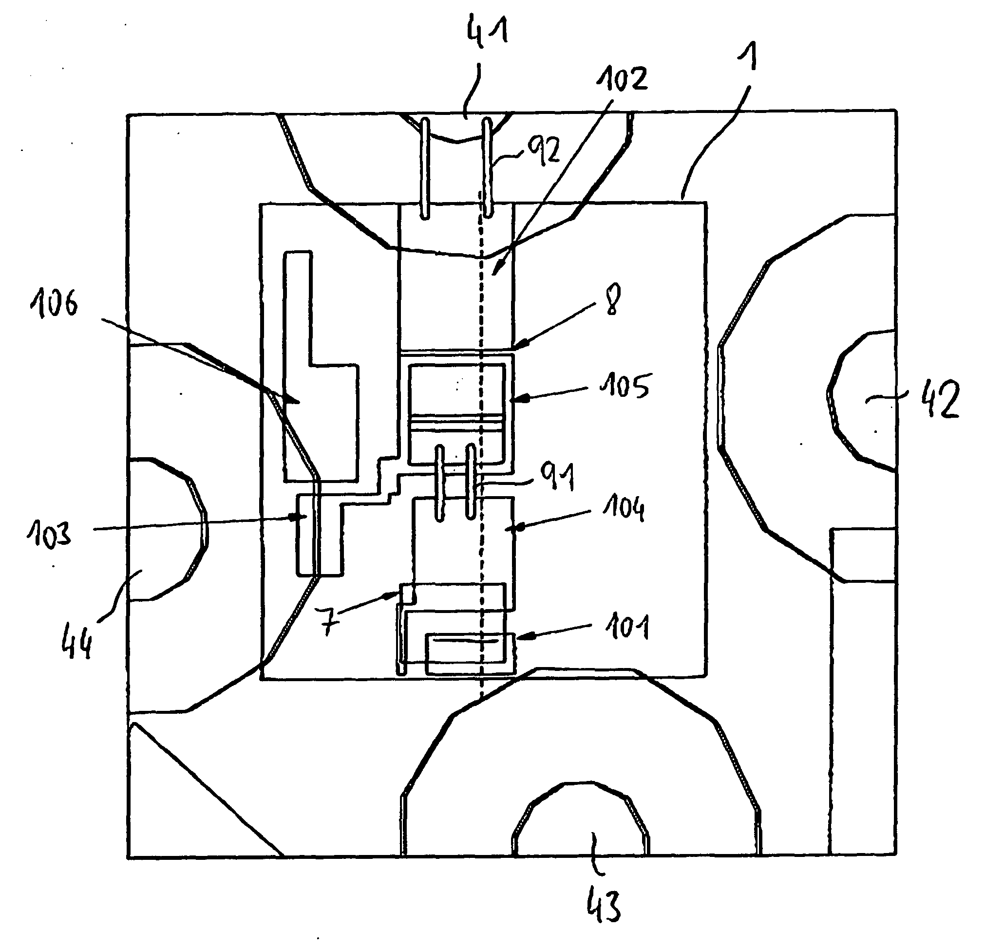
[0009] Using the carrier substrate for contacting the contact of the semiconductor component that is subjected to the reference voltage makes it possible to dispense with a high-frequency pin and consequently to provide a drastic reduction in the overall bonding wire length in the high-frequency path. The parasitic inductances occurring can be considerably reduced as a result, so that there is an improved HF performance into the frequency range greater than 5 GHz, even when a semiconductor component of low impedance in the range between 20 and 30 ohms is used.
[0016] In a further preferred configuration, the matching resistor has a negative temperature coefficient. Such a configuration is favorable in particular when the semiconductor component is formed as a semiconductor laser, since a semiconductor laser demands a higher modulation current at increased operating temperatures. This can be achieved, or at least assisted, by a matching resistor with a negative temperature coefficient. A matching resistor with a negative temperature coefficient is provided, for example, by a boron-doped polysilicon resistor.
[0019] In an advantageous configuration, the first contact of the semiconductor component, on which the reference voltage is present, is connected via a short-circuiting element to the first contacting region of the carrier substrate. The short-circuiting element is in this case only attached during the production of the transmitting and / or receiving device on a wafer after a burn-in. The short-circuiting element is, for example, a piece of solder or a soldered block (jumper). The short-circuiting element has the effect of “activating” a short-circuit with respect to the reference voltage which is present on the first contacting region via the electrically conducting carrier substrate.

Problems solved by technology

However, at data rates of 10 Gbits / s, rates which have by now been accomplished, the high-frequency (HF) performance deteriorates, since the impedance of the fed-in bonding wires plays an increasingly disadvantageous role with increasing frequency.
It has been found that the HF properties of an optical transmitting and / or receiving device are substantially limited by the resultant inductance of the bonding wires, which at frequencies of about 10 Gbit / s is of the order of magnitude of 1 to 1.5 nH (1 nH=1 henry).
On account of their inductance, the bonding wires provide a reactance, which is connected in series with the effective resistance of a semiconductor laser of typically 5 ohms, which leads to a change in impedance and an undesired signal reflection.
The problem is intensified by the fact that the appearance of the standard IEEE 802.3ae (10 Gbit Ethernet) and the associated requirements for very compact modules with low power consumption makes it likely that a 50 ohms impedance of the laser module is not viable in the long term for reasons of the power demand, so that it is desirable to change over to a smaller impedance of 20 to 30 ohms.
With a smaller impedance of the driver system, however, the sensitivity of the construction to parasitic inductances increases, i.e. the reactance component caused by the inductance of the bonding wires becomes more noticeable and leads to an increased reflection of the high-frequency signal.

Method used


Image

  • Optical transmission and/or receiving device
  • Optical transmission and/or receiving device
  • Optical transmission and/or receiving device

Examples


Embodiment Construction

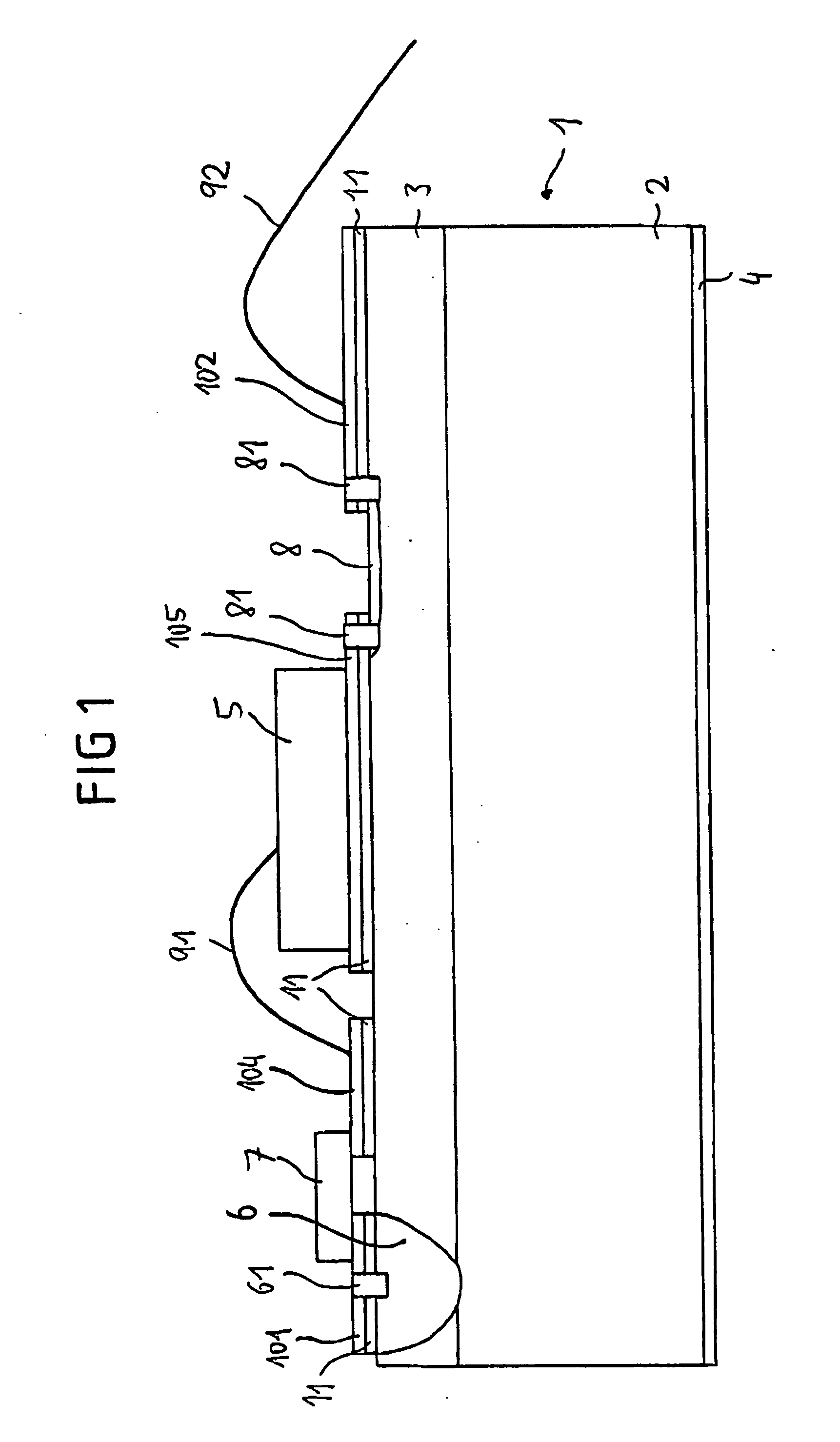
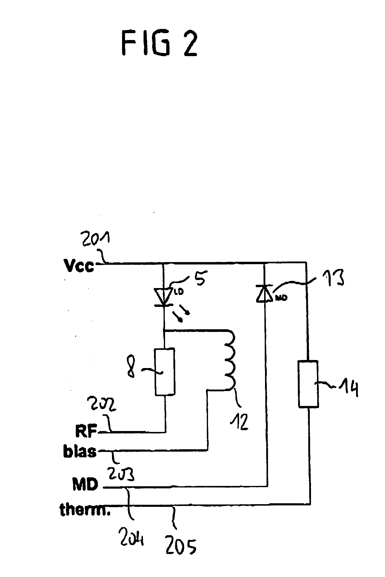
[0031] FIGS. 1 to 4 show an exemplary embodiment of an optical transmitting device with a semiconductor chip 5, which is arranged on a carrier substrate 1, also referred to as the submount.

[0032]FIG. 1 shows a sectional representation of the submount 1 with the elements arranged on it. The submount 1 comprises a highly conducting silicon substrate 2 and a high-ohmic, low-doped silicon epitaxial layer 3 arranged on it. The silicon substrate 2 preferably has in this case a resistance of between 0.05 and 0.2 ohm-cm, in particular of 0.01 ohm-cm, and a thickness of between 300 and 400 μm, in particular of about 360 μm. The epitaxial layer 3 has a resistance of preferably greater than 20 ohm-cm, in particular of 100 ohm-cm, and a thickness of 30 to 50 μm, in particular of 40 μm. On the underside of the silicon substrate 2 there is a large-area rear metallization 4, which is, for example, adhesively bonded or soldered onto a TO base plate, as will be explained in more detail on the basis...


PUM


Abstract

The invention relates to an optical transmitting and / or receiving device, having: a semiconductor component with a first contact for connection with a reference voltage and a second contact for applying or leading away a high-frequency electrical signal; an electrically conducting carrier substrate with a first surface and a second surface, the semiconductor component being arranged on the first surface of the carrier substrate, the second surface of the carrier substrate having a metallization which can be connected to the reference voltage, and the reference voltage being applied by an electrical path through the carrier substrate to a first contacting region of the first surface of the carrier substrate, and the first contact of the semiconductor component being electrically connected to the first contacting region.

Description

[0001] The invention relates to an optical transmitting and / or receiving device, as used in optical telecommunications engineering. It relates in particular to a construction of an optical transmitting and or receiving device which is distinguished by favorable high-frequency properties. A preferred field of use is that of directly modulated semiconductor lasers in the frequency range greater than 5 GHz and associated receiving devices with a photodiode. BACKGROUND OF THE INVENTION [0002] U.S. Pat. No. 6,271,049 B1 and EP 0 660 467 A1 disclose optical components with a laser chip as the light transmitter. The laser chip is arranged on a carrier consisting of silicon, which can be mounted on the base plate of a TO package. The contacting of the laser chip takes place via bonding wires. [0003] The known optical components exhibit good high-frequency properties and data rates of up to about 2.5 Gbits / s. However, at data rates of 10 Gbits / s, rates which have by now been accomplished, th...

Claims


Application Information

Patent Timeline
IPC IPC(8): H01L21/00H01L33/00
CPCH01S5/02248H01S5/02276H01S5/06832H01L2224/48091H01L2924/00014H01L2924/3011H01L2924/00H01L2924/30107H01S5/02325H01S5/02345
Inventor REZNIK, DANIELSTIER, OLIVERRING, MELANIEKUHLMANN, WERNERPRODINGER, BENJAMINIWANOWSKI, NICOLA
Owner II VI DELAWARE INC
Learn More