Physical vapor deposition plasma reactor with RF source power applied to the target and having a magnetron

a plasma reactor and vapor deposition technology, applied in vacuum evaporation coating, cables, coatings, etc., can solve the problems of consuming production time, high production cost, adding cost, and entail some additional expens

Active Publication Date: 2006-08-03
APPLIED MATERIALS INC
View PDF98 Cites 93 Cited by
  • Summary
  • Abstract
  • Description
  • Claims
  • Application Information

AI Technical Summary

Problems solved by technology

Because copper tends to diffuse over time through the insulator layer to cause catastrophic short circuiting, a barrier layer that blocks copper diffusion is placed between the copper material and the dielectric material wherever the two materials interface in the integrated circuit.
A problem arises in forming the vias extending vertically between the horizontal interconnect layers, as follows.
The interruption represented by the selective removal of the barrier layer entails a higher production cost and consumes production time.
While this dual-purpose reactor works extremely well, it does entail some additional expense.
In order to avoid process contamination, the re-sputtering coil is formed of pure tantalum, adding cost.
One problem is that the metal vapor deposition process can coat the ceiling with metal and thereby block inductive coupling from the coil antenna.
A more significant problem is that the RF plasma produced by the coil produces a high proportion of metal ions from the target, so that the wafer bias cannot be optimized for etch selectivity to horizontal surfaces without impacting (de-optimizing) the flux of metal ions/vapor from the target.
Typically, however, are large share of the copper ions are deposited on shields in the chamber

Method used


Image

  • Physical vapor deposition plasma reactor with RF source power applied to the target and having a magnetron
  • Physical vapor deposition plasma reactor with RF source power applied to the target and having a magnetron
  • Physical vapor deposition plasma reactor with RF source power applied to the target and having a magnetron

Examples


Embodiment Construction

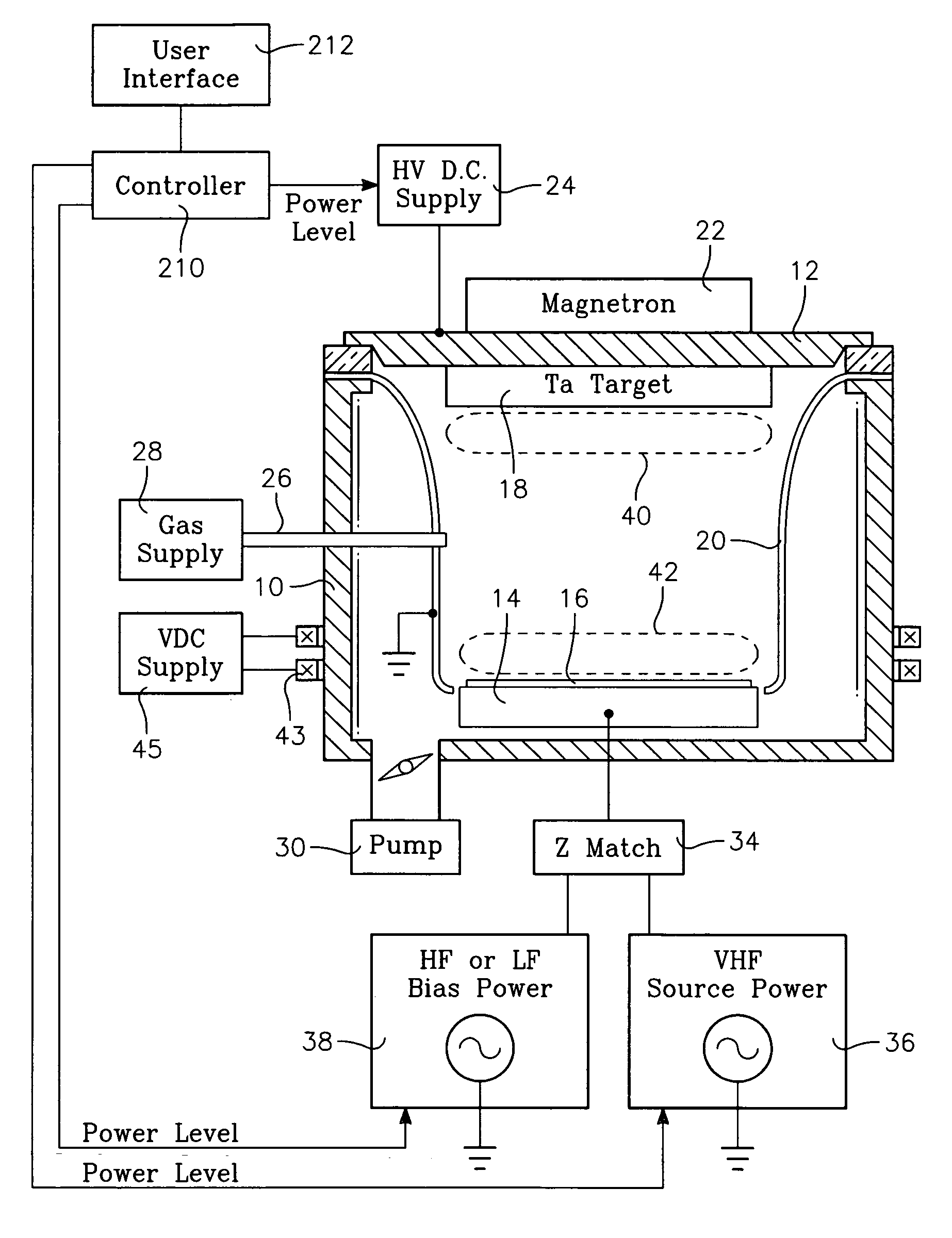
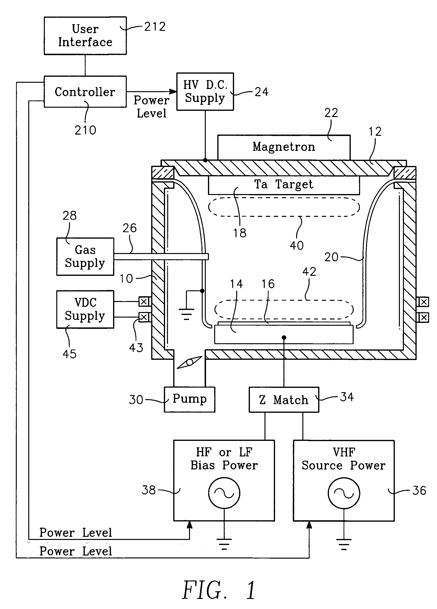
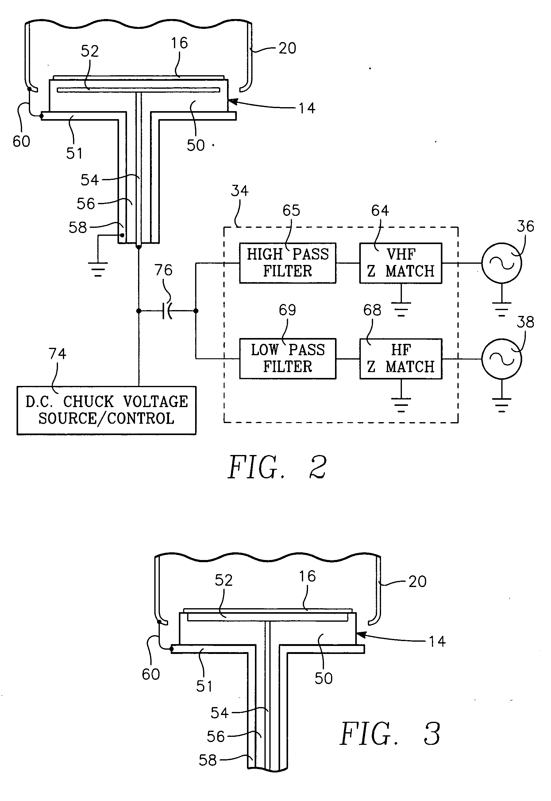
[0040] A plasma reactor forms barrier layers (such as a tantalum / tantalum nitride film or titanium / titanium nitride film) for conductors (such as copper, for which the barrier should be tantalum / tantalum nitride) in trenches or through vias between successive interconnection layers of an integrated circuit. The plasma reactor is capable of both physical vapor deposition and of highly selective re-sputtering to remove barrier material from the exposed horizontal surfaces of the underlying conductor constituting the floor of the via. Significantly, the reactor accomplishes all this without an internal coil that had previously been required for a fully and precisely controllable re-sputtering step. Instead, a plasma is formed near the wafer to perform the re-sputtering step. For this purpose a process gas such as argon may be introduced and source power is applied to the wafer at an RF frequency effective for capacitively coupling energy to kinetic electrons to excite argon plasma ions...


PUM

PropertyMeasurementUnit
Diameteraaaaaaaaaa
Frequencyaaaaaaaaaa
Lengthaaaaaaaaaa

Abstract

A physical vapor deposition reactor includes a metal sputter target, a D.C. sputter power source coupled to the metal sputter target and a wafer support pedestal facing the metal sputter target. A movable magnet array is adjacent a side of the metal sputter target opposite the wafer support pedestal. A solid metal RF feed rod engages the metal sputter target and extends from a surface of the target on a side opposite the wafer support pedestal. A VHF impedance match circuit is coupled to an end of the RF feed rod opposite the metal sputter target and a VHF RF power generator coupled to said VHF impedance match circuit. Preferably, the reactor of further includes a center axle about which the movable magnet array is rotatable, the center axle having an axially extending hollow passageway, the RF feed rod extending through the passageway.

Description

CROSS-REFERENCE TO RELATED APPLICATIONS [0001] This application is a continuation-in-part of U.S. application Ser. No. 11 / 052,011 filed Feb. 3, 2005, entitled “APPARATUS FOR METAL PLASMA VAPOR DEPOSITION AND RE-SPUTTER WITH SOURCE AND BIAS POWER FREQUENCIES APPLIED THROUGH THE WORKPIECE” by Karl M. Brown et al. and assigned to the present assignee.BACKGROUND OF THE INVENTION [0002] With recent technological advances in integrated circuit design, there are now as many as six to ten interconnect layers of a multilayer interconnect structure overlying the semiconductor transistors. Insulator layers separate the successive conductor layers. The conductor interconnect layers can have completely different conductor patterns and are connected to one another and to the transistor layer at different locations through vias extending vertically through the insulator layers. It is the formation of the vias with which the present invention is concerned. [0003] To reduce resistive power losses in...

Claims


Application Information

Patent Timeline
IPC IPC(8): C23C14/00
CPCC23C14/046C23C14/345C23C14/358H01J37/32082H01L21/76844H01J37/3408H01L21/2855H01L21/76843H01J37/32706
Inventor BROWN, KARL M.PIPITONE, JOHNMEHTA, VINEET
Owner APPLIED MATERIALS INC
Why Eureka
Try Eureka