Nonvolatile memory device made of resistance material and method of fabricating the same

a technology of resistance material and memory device, which is applied in the direction of semiconductor devices, basic electric elements, electrical appliances, etc., can solve the problems of reducing productivity of conventional nonvolatile memory devices, difficult to etch resistors, and long time to etch resistors, so as to increase the integration of memory devices, reduce the size of data storage layers, and ensure the effect of storage performan

Active Publication Date: 2006-08-03
SAMSUNG ELECTRONICS CO LTD
View PDF26 Cites 102 Cited by
  • Summary
  • Abstract
  • Description
  • Claims
  • Application Information

AI Technical Summary

Benefits of technology

[0013] According to embodiments of the present invention, a three-dimensional data storage layer may be obtained. Because of this three-dimensional structure, the size of the data storage layer may be reduced, while the storage performance is not degraded. Also, the three-dimensional data storage layer may increase integration of the memory device and decrease a reset current (Ireset), which is preferred in data write and erase operation.

Problems solved by technology

Thus, when using a conventional DRAM process, it is difficult to etch the resistor and, even though this is possible, it takes a long time to etch the resistor.
For these reasons, conventional nonvolatile memory devices have reduced productivity, increased manufacturing costs and as a result are uncompetitive in markets.
Also, since the resistors of the conventional nonvolatile memory devices are formed of a thin film type using physical vapor deposition (PVD), it is difficult to obtain a dense and uniform layer quality.
It is also difficult to control a composition ratio of elements constituting the resistors, which can have a great influence on the switching characteristics of the memory devices.
The MOCVD method has a limitation in controlling the oxygen content.
Also, since the metal-containing layer has a thin film shape, the high integration potential and reduction of reset current ability are limited.

Method used


Image

  • Nonvolatile memory device made of resistance material and method of fabricating the same
  • Nonvolatile memory device made of resistance material and method of fabricating the same
  • Nonvolatile memory device made of resistance material and method of fabricating the same

Examples


Embodiment Construction

[0022] Embodiments of the present invention will now be described more fully with reference to the accompanying drawings, in which exemplary embodiments of the invention are shown.

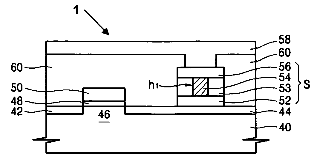
[0023]FIG. 1 is a schematic sectional view of a nonvolatile memory device 1 using resistance material according to a preferred embodiment of the present invention;

[0024] Referring to FIG. 1, the nonvolatile memory device 1 using the resistance material includes a substrate 40, a transistor formed on the substrate 40, and a data storage part S connected to a portion of the transistor. The transistor includes a source 42, a drain 44, and a gate stack structure formed on a channel region 46 between the source 42 and the drain 44. The source 42 and the drain 44 may be formed of doped conductive impurities. The gate stack structure includes a gate insulating layer 48 and a gate electrode 50, which are stacked in sequence. The transistors are one example of a suitable structure. A switching diode may also be p...


PUM


Abstract

A nonvolatile memory device using a resistance material and a method of fabricating the same are provided. The nonvolatile memory device includes a switching element, and a data storage part electrically connected to the switching element. In the data storage part, a lower electrode is connected to the switching element, and an insulating layer is formed on the lower electrode to a predetermined thickness. The insulating layer has a contact hole exposing the lower electrode. A data storage layer is filled in the contact hole and the data storage layer is formed of transition metal oxide. An upper electrode is formed on the insulating layer and the data storage layer.

Description

CROSS-REFERENCE TO RELATED PATENT APPLICATION [0001] This application claims the benefit of Korean Patent Application No. 10-2005-0008752, filed on Jan. 31, 2005, in the Korean Intellectual Property Office, the disclosure of which is expressly incorporated herein in its entirety by reference. BACKGROUND OF THE INVENTION [0002] 1. Field of the Invention [0003] Embodiments of the present invention relate to a nonvolatile memory device made of resistance material and a method of fabricating the same, and more particularly, to a nonvolatile memory device capable of providing high integration and reducing a reset current and a method of fabricating the same. [0004] 2. Description of the Related Art [0005] Ferroelectric RAM (FRAM), magnetic RAM (MRAM) and phase-change RAM (PRAM) are nonvolatile memory devices made of resistance material. While DRAM or flash memory stores binary data using charges, FRAM, MRAM and PRAM store binary data using a polarization characteristic of a ferroelectric...

Claims


Application Information

Patent Timeline
Patent Type & Authority Applications(United States)
IPC IPC(8): H01L29/76
CPCH01L45/1616H01L45/1683H01L45/04H01L45/1233H01L45/146H01L27/2436H10B63/30H10N70/20H10N70/023H10N70/066H10N70/8833H10N70/826H01L21/76897
Inventor LEE, JUNG-HYUNCHOI, SUNG-KYUKIM, KYU-SIK
Owner SAMSUNG ELECTRONICS CO LTD
Why Eureka
Try Eureka