Semiconductor device

Active Publication Date: 2006-08-03
MITSUBISHI ELECTRIC CORP
View PDF1 Cites 15 Cited by
  • Summary
  • Abstract
  • Description
  • Claims
  • Application Information

AI Technical Summary

Benefits of technology

[0009] As described above, according to the semiconductor device of the present invention, it is possible to prevent t

Problems solved by technology

There are problems, however, that it is difficult to irradiate the electron beam locally to the peripheral part of the diode, and that this irradiation step makes the product process complicate.
In the case that

Method used


Image

  • Semiconductor device
  • Semiconductor device
  • Semiconductor device

Examples


embodiment 1

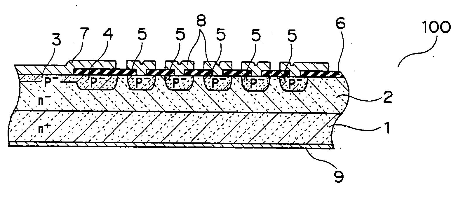
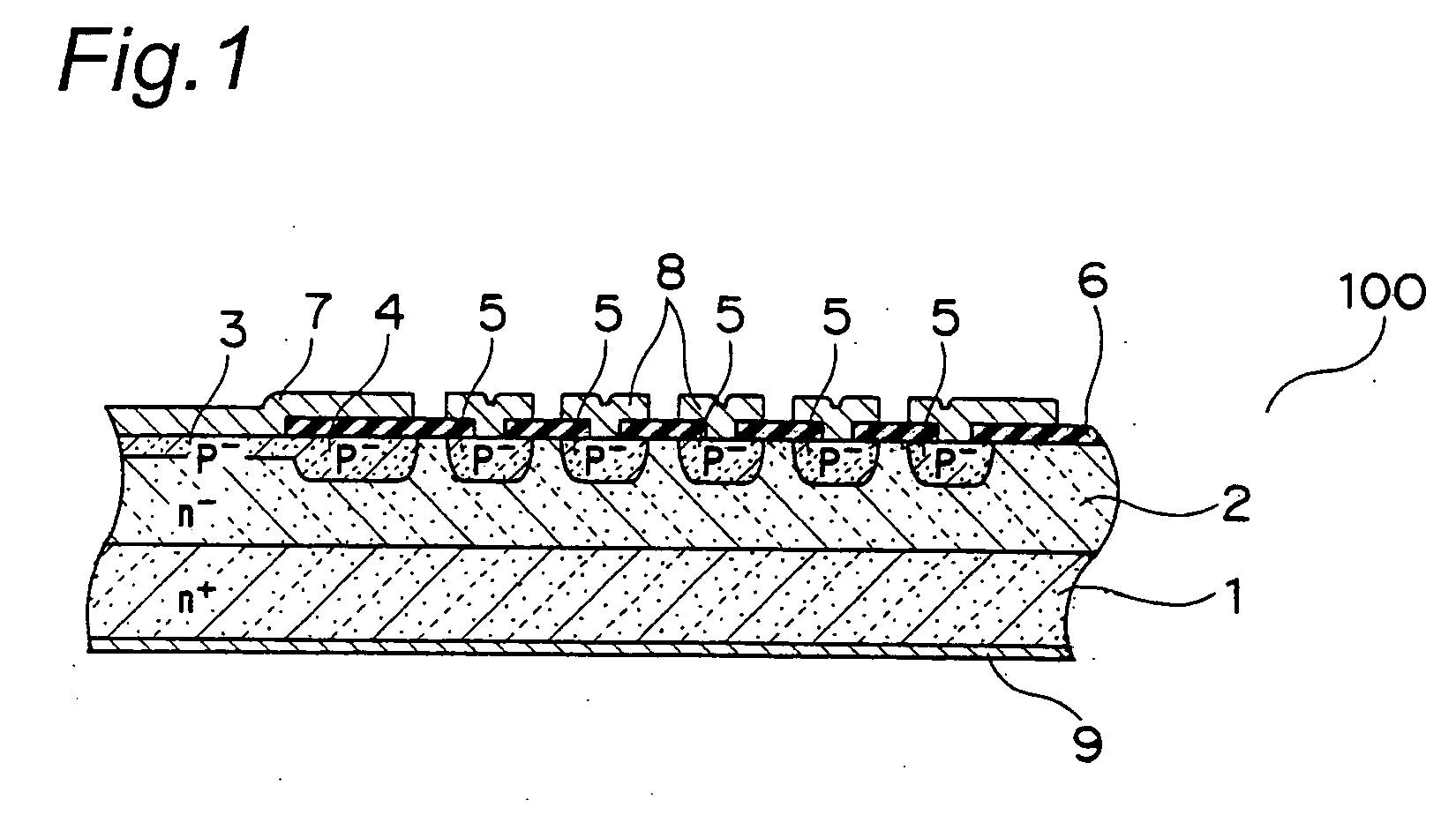
[0017]FIG. 1 shows a sectional view of a diode according to the embodiment 1 of the present invention generally denoted at 100. The diode 100 includes an n-type semiconductor substrate 1 of silicon for instance. On the semiconductor substrate 1, an n-type n− semiconductor layer 2 is formed. On the front surface of the n− semiconductor layer 2, a p-type anode region (base region) 3 is formed.

[0018] Around the anode region 3, p-type anode peripheral region (base peripheral region) 4 connected to the anode region is formed. The concentration of the p-type impurity in the anode peripheral region 4 is less than that in the anode region 3. Further, the depth of the anode peripheral region 4 is more than that of the anode region 3. Also it is noted that, in the diode 100, the depth of the anode peripheral region 4 is substantially constant, and the bottom face of that is substantially flat.

[0019] Furthermore, a p-type guard ring region 5 is formed to surround the anode region 3. In FIG. ...

embodiment 2

[0041]FIG. 7 shows a sectional view of a diode according to the embodiment 2 of the present invention generally denoted at 200. In FIG. 7, the numerals which are identical with those of FIG. 1 denote identical or corresponding components. In the diode 200, the oxide film 6 covers the right half of the cathode peripheral regions 4, on the other hand, in the diode 100, the oxide film 6 covers the all of the cathode peripheral regions 4. This is the difference between the diodes 100 and 200, and hereby, the diode 200 has the structure including the cathode electrode 17 which extends over the cathode peripheral region 4. The other components of the diode 200 are substantially the same as those of the diode 100.

[0042] The concentration of the p-type impurity of the cathode peripheral region 4 is lower than that of the cathode region 3 (Namely, the value of the resistance of the cathode peripheral region 4 is higher than that of the cathode region 3). Hereby the injunction of holes into ...


PUM


Abstract

A semiconductor device, including: a semiconductor substrate of the first conductivity type having a first surface and a second surface; a base region of the second conductivity type formed on the first surface of the semiconductor substrate; a guard ring region of the second conductivity type formed around the base region, and having the second type impurity of which concentration is lower than that of the base region; a first electrode formed on the base region; and a second electrode formed on the second surface of the semiconductor substrate, further including a base peripheral region formed around the base region and being connected to the base region, wherein the base peripheral region is deeper than the base region and has the substantially constant depth, and the concentration of the second conductivity type impurity included in the base peripheral region is lower than that included in the base region.

Description

BACKGROUND OF THE INVENTION [0001] 1. Field of the Invention [0002] The present invention relates to a semiconductor device, and more particularly, to a diode having low forward voltage drop (Vf) and preventing recovery breakdown in case of reverse recovery. [0003] 2. Description of the Related Art [0004] Recently, a converter bridge having a high power IGBT and a diode disposed in parallel is used for a converter circuit. In the diode, an n− semiconductor layer sandwiched between a p semiconductor layer as an anode and n+ semiconductor layer as a cathode is designed to have long lifetime of carriers in order to decrease the forward voltage. In the event that the lifetime of carriers in the n− semiconductor layer is long like this, recovery current occurred when the diode is switched from the on-state to the off-state (recovery process) is increased. Hereby, there arises a problem that the diode is destroyed during the recovery process (recovery breakdown). Specially, the recovery b...

Claims


Application Information

Patent Timeline
IPC IPC(8): H01L27/082
CPCH01L29/0619H01L29/404H01L29/8611E04G7/12E04G7/34E04G1/08
Inventor TAKAHASHI, HIDEKI
Owner MITSUBISHI ELECTRIC CORP
Why Eureka
Try Eureka