Organic electroluminescent display apparatus and method of fabricating the same

a technology of electroluminescent display and organic electroluminescent devices, which is applied in the direction of discharge tube/lamp details, discharge tube luminescnet screens, other domestic articles, etc., can solve the problems of narrowed deviation of mask position, and degradation of product yield, so as to prevent the reduction of the effective light emitting area, the yield can be improved, and the required positioning accuracy is alleviated

Active Publication Date: 2006-08-03
SANYO ELECTRIC CO LTD
View PDF10 Cites 43 Cited by
  • Summary
  • Abstract
  • Description
  • Claims
  • Application Information

AI Technical Summary

Benefits of technology

[0012] An object of this invention is to provide an organic electroluminescent display apparatus wherein the required accuracy of positioning the organic electroluminescent devices is alleviated, so that the yield can be improved, the effective light emitting area can be prevented from being reduced, and the uniform light emitting properties can be ensured, and a method of fabricating the same.

Problems solved by technology

However, deviation of the position of the mask may be caused in deposition of organic material layers using the mask having apertures corresponding to respective pixel.
This deviation of the position of the mask may then lead to deviation of the positions of the organic material layers such as light emitting layers, consequently resulting in the narrowed effective light emitting area and the degradation of the yield of a product.
Furthermore, the thickness of the organic material layers may become ununiform due to the shadowing from end portions of the apertures of the mask.
This not only prevents the uniform light emitting properties, but causes the effective light emitting area to be reduced.

Method used


Image

  • Organic electroluminescent display apparatus and method of fabricating the same
  • Organic electroluminescent display apparatus and method of fabricating the same
  • Organic electroluminescent display apparatus and method of fabricating the same

Examples


Embodiment Construction

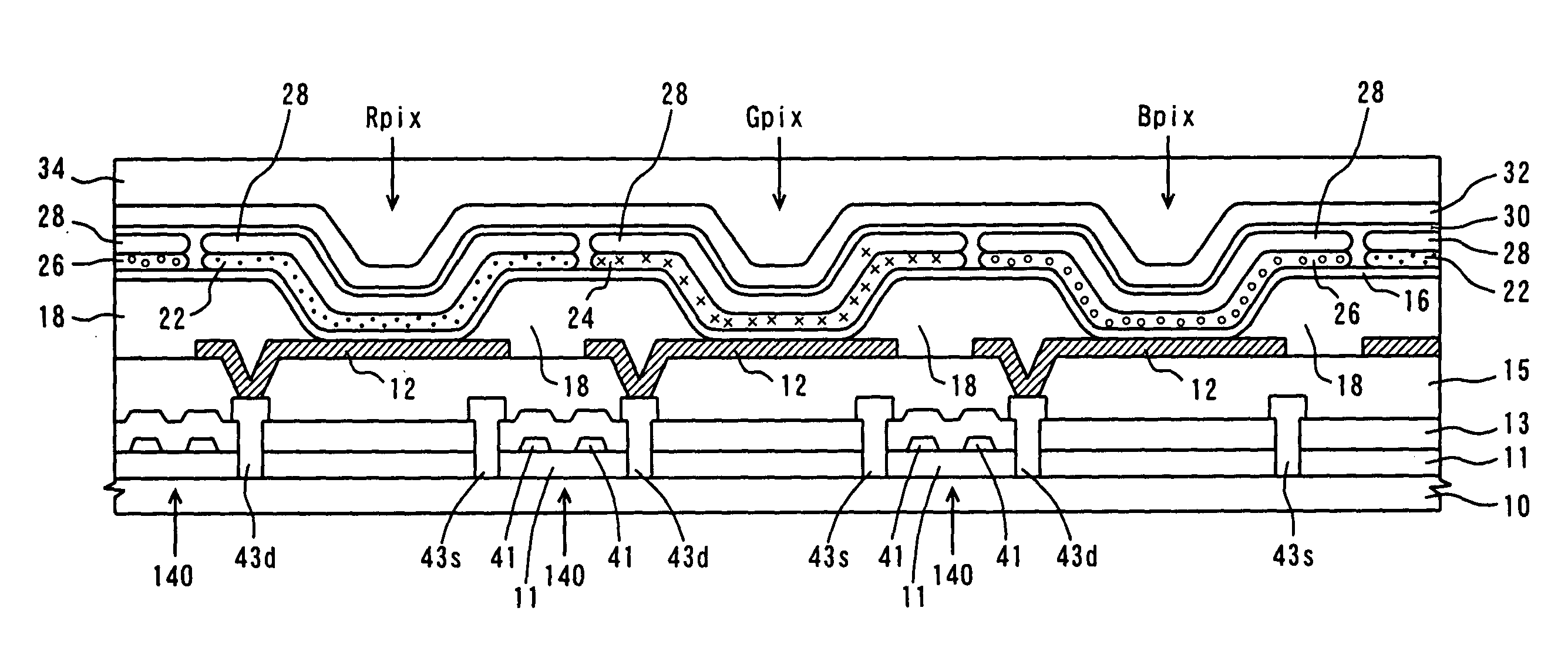
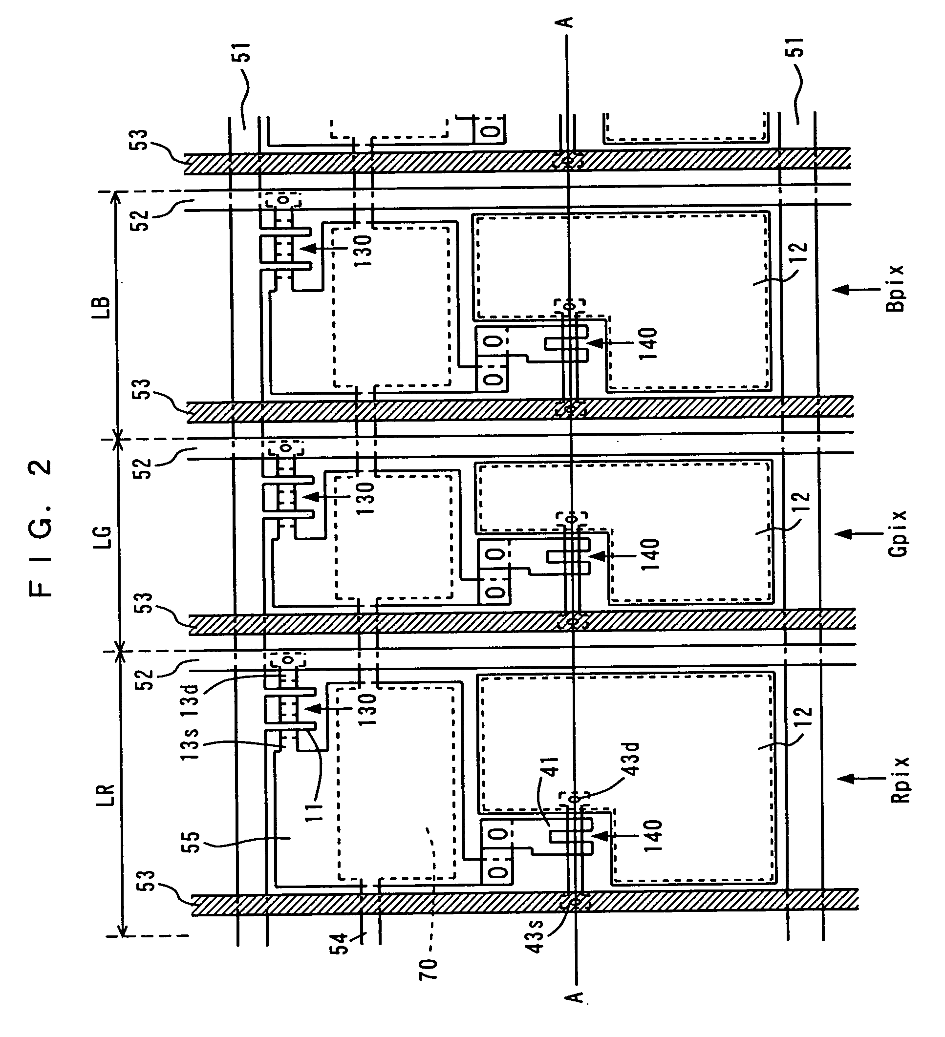
[0038] Description is now made of an organic electroluminescent display apparatus (hereinafter referred to as an organic EL display apparatus) according to an embodiment of the present invention.

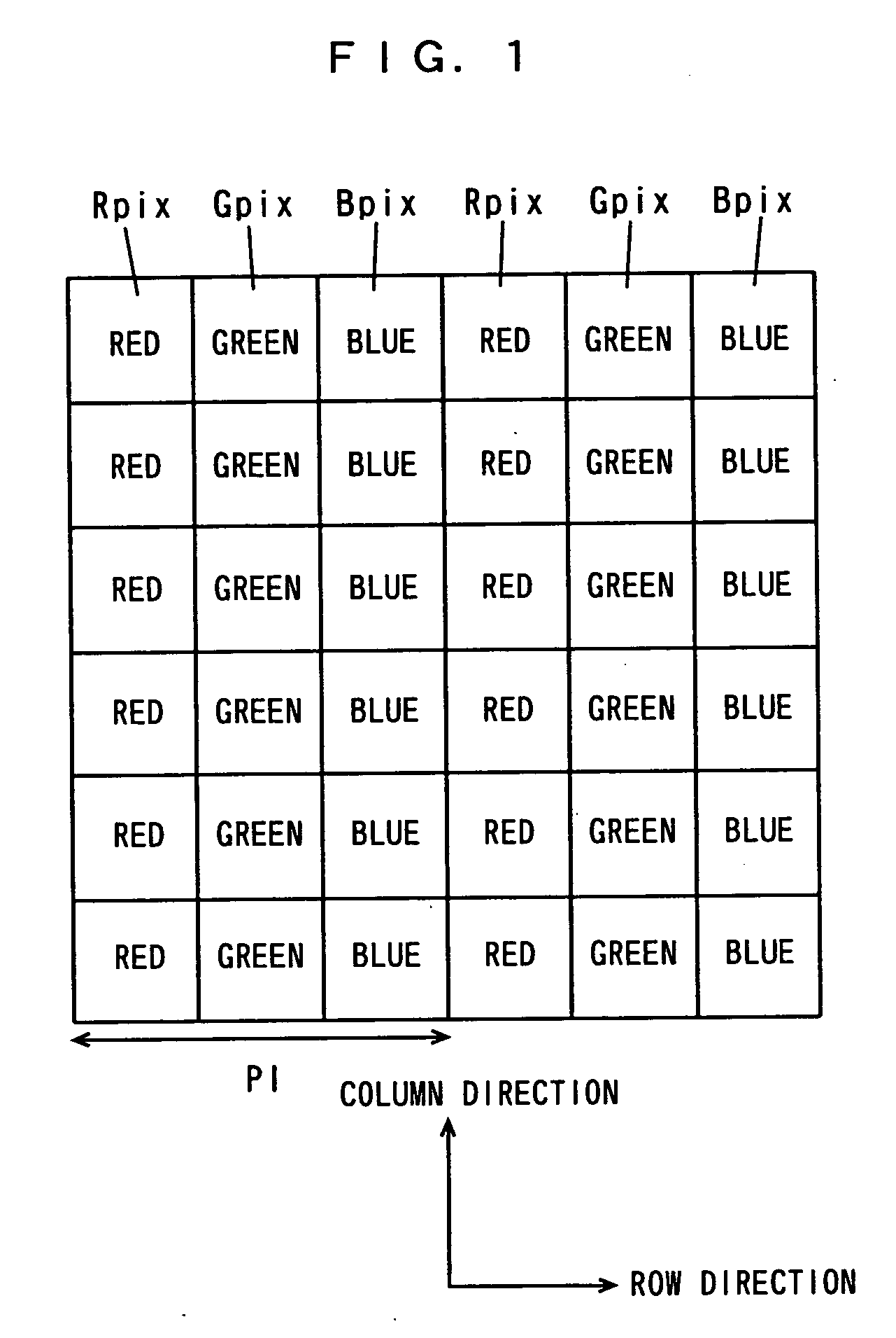
[0039]FIG. 1 is a schematic plan showing the arrangement of pixels of an organic EL display apparatus according to one embodiment of the present invention. Organic EL display apparatuses are composed of a plurality of organic electroluminescent devices (hereinafter referred to as organic EL devices).

[0040] In the organic EL display apparatus shown in FIG. 1, Rpix, which are pixels emitting red light (hereinafter referred to as R pixels), Gpix, which are pixels emitting green light (hereinafter referred to as G pixels), and Bpix, which are pixels emitting blue light (hereinafter referred to as B pixels) are arranged in the form of a matrix.

[0041] R pixels Rpix are composed of the organic EL devices emitting red light, G pixels Gpix are composed of the organic EL devices emitting green ligh...


PUM


Abstract

The light emitting layers and the electron transporting layers of R pixels, G pixels, and B pixels are formed to have a stripe shape extending in the column direction. The red light emitting layer and the electron transporting layer in R pixels are formed to be continuous layers using the same mask in a first vapor deposition chamber, the green light emitting layer and the electron transporting layer of G pixels are formed to be continuous layers using the same mask in a second vapor deposition chamber, and the blue-white light emitting layer and the electron transporting layer of B pixels are formed to be continuous layers using the same mask in a third vapor deposition chamber.

Description

BACKGROUND OF THE INVENTION [0001] 1. Field of the Invention [0002] The present invention relates to an organic electroluminescent display apparatus comprising a plurality of organic electroluminescent devices and a method of fabricating the same. [0003] 2. Description of the Background Art [0004] Organic electroluminescent display apparatuses (hereinafter abbreviated to organic EL display apparatuses) are expected to be promising as display apparatuses in place of liquid crystal display apparatuses currently in widespread use, and the development for practical utilization is under way. In particular, active matrix organic EL display apparatuses comprising Thin Film Transistors (TFTs) as switching devices in respective pixels are capable of having larger screens and higher definition because of holding display data in each pixel, and are considered to be the leading apparatuses among the next generation flat panel displays. [0005] An organic EL display apparatus includes a plurality...

Claims


Application Information

Patent Timeline
Patent Type & Authority Applications(United States)
IPC IPC(8): H01L51/50H05B33/00H01L27/32H01L51/00H05B33/12H01L51/56H05B33/10H05B33/14H05B33/22
CPCH01L27/3211H01L27/3244H01L51/0054H01L51/0058H01L51/0059H01L51/006H01L51/0071H01L51/0072H01L51/0081H01L51/56Y10S428/917H10K59/35H10K59/12H10K85/622H10K85/626H10K85/633H10K85/631H10K85/324H10K85/657H10K85/6572H10K71/00H05B33/10
Inventor KANNO, HIROSHIHAMADA, YUJIMATSUKI, HIROSHINISHIO, YOSHITAKA
Owner SANYO ELECTRIC CO LTD
Why Eureka
Try Eureka