Electronics device, optical panel, inspection probe, inspection device for the optical panel and inspection method for the optical panel
- Summary
- Abstract
- Description
- Claims
- Application Information
AI Technical Summary
Benefits of technology
Problems solved by technology
Method used
Image

Examples
first exemplary embodiment
1 First Exemplary Embodiment
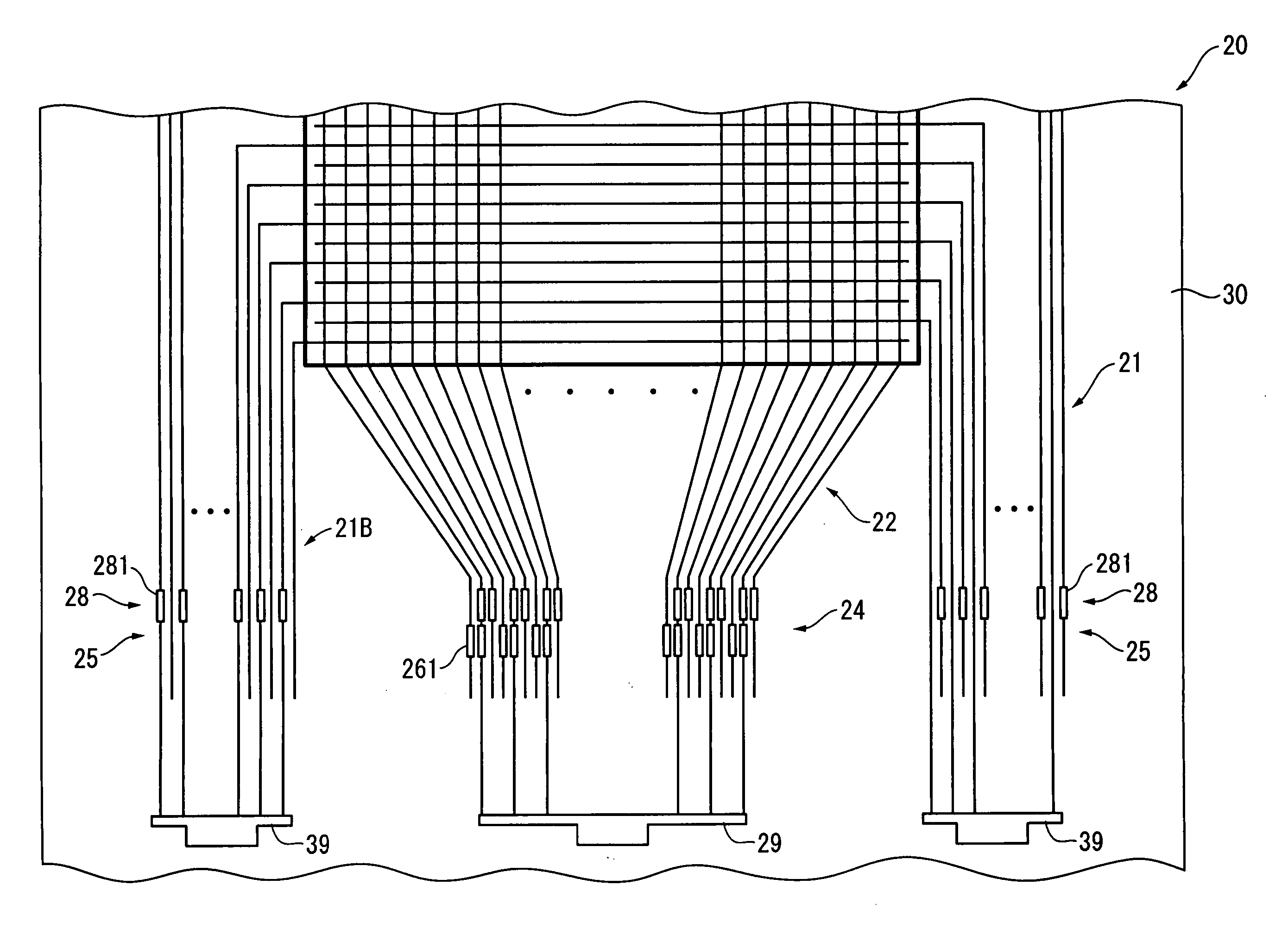
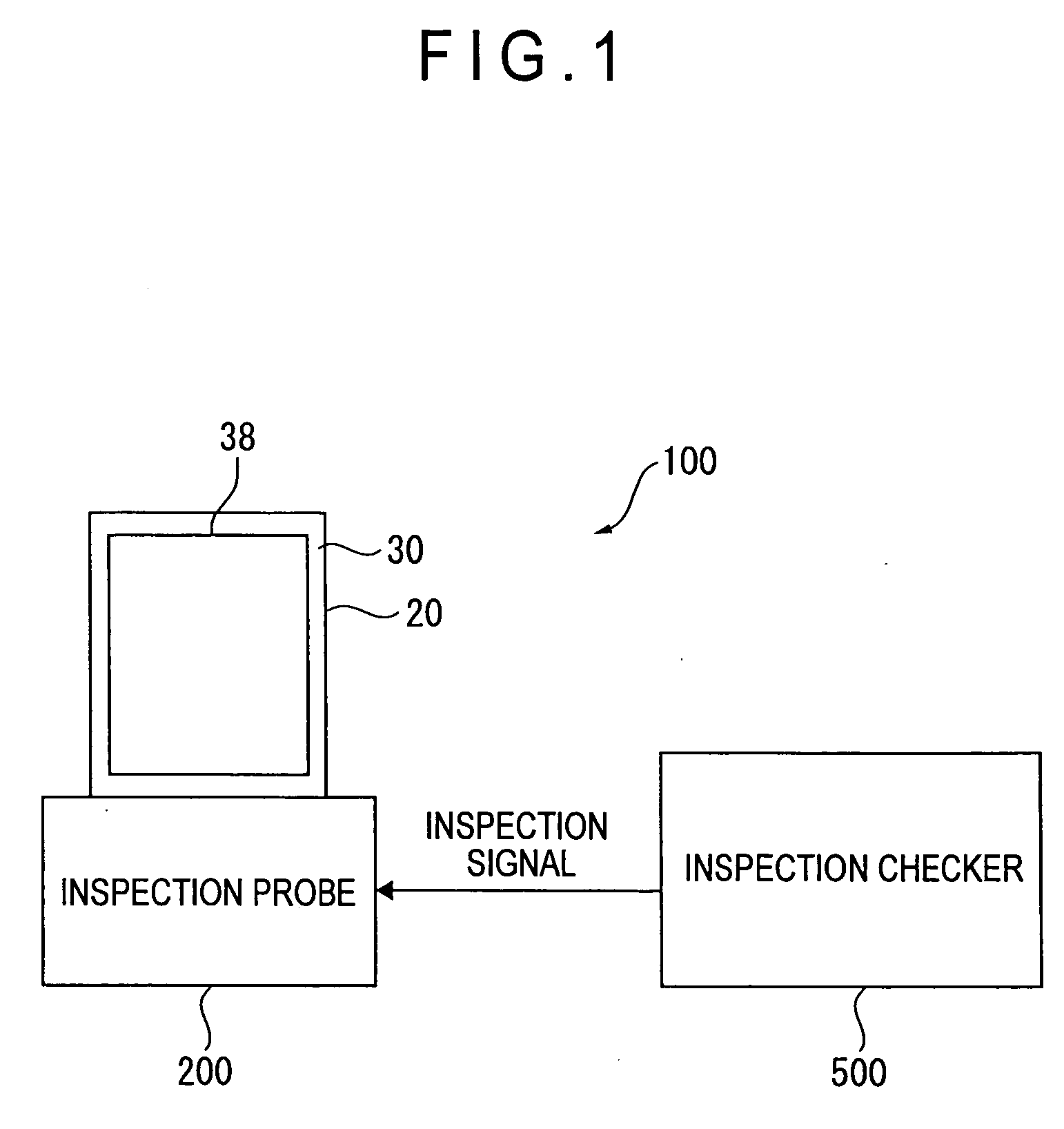
[0100] A first exemplary embodiment of an optical panel and an inspection device for inspecting the optical panel according to the invention will be described with reference to FIGS. 1 to 6.
[0101]FIG. 1 shows an overall layout in which a liquid crystal display panel 20 as the optical panel is connected in an inspection device 100.
[0102] An inspection probe 200 is connected at a side of a substrate 30 of the liquid crystal display panel 20. An inspection signal is input from an inspection checker (inspection signal transmitter) 500 via the inspection probe 200 to the liquid crystal display panel 20. An image display inspection of the liquid crystal display panel 20 is conducted by judging a light-on state of the thus lighted liquid crystal display panel 20.
[0103] First, the liquid crystal display panel 20 to be inspected and an outline of the inspection of the liquid crystal display panel 20 will be described.
[0104] In the image display inspection of t...
second exemplary embodiment
2 Second Exemplary Embodiment
[0158] Next, a second exemplary embodiment of the optical panel according to the invention will be described with reference to the FIG. 7.
[0159] Although basic arrangements of the liquid crystal display panel of the second exemplary embodiment are similar to those of the liquid crystal display panel of the first exemplary embodiment, the second exemplary embodiment has a feature that an electric conductor is layered on the data lines being exposed as a signal input terminal in the inspection terminal allocating layer.
[0160]FIG. 7 is a cross section showing a connection state where the red wiring portion 300R of the inspection probe 200 is connected with the red-terminal allocating layer 26R in the drawing portion 24 of the data lines 22.
[0161] Regarding the red-terminal allocating layer 26R, the green data lines 22G and the blue data lines 22B, except for the red data lines 22R, are covered by the insulating film 261.
[0162] On the other hand, the red...
third exemplary embodiment
3 Third Exemplary Embodiment
[0167] A third exemplary embodiment of the invention will be described with reference to the FIGS. 8 and 9.
[0168] Although basic arrangements of the third exemplary embodiment are similar to those of the first exemplary embodiment, the third exemplary embodiment has features that the inspection terminal allocating layer is also provided for the drawing portion 25 of the scanning lines 21 and that the inspection probe 200 is provided with the wiring portions 300R, 300G, 300B that are connected with the inspection terminal allocating layers 26R, 26G, 26B of the scanning lines 21.
[0169]FIG. 8 shows an arrangement of the liquid crystal display panel of the third exemplary embodiment. FIG. 9 shows an arrangement of the inspection probe of the third exemplary embodiment.
[0170] In FIG. 8, the drawing portion 24 of the data lines 22 is provided with the inspection terminal allocating layers 26R, 26G, 26B.
[0171] The drawing portions 25 of the scanning lines 21...
PUM
 Abstract
Description
Claims
Application Information
 - Generate Ideas
- Intellectual Property
- Life Sciences
- Materials
- Tech Scout
- Unparalleled Data Quality
- Higher Quality Content
- 60% Fewer Hallucinations
Browse by: Latest US Patents, China's latest patents, Technical Efficacy Thesaurus, Application Domain, Technology Topic, Popular Technical Reports.
© 2025 PatSnap. All rights reserved.Legal|Privacy policy|Modern Slavery Act Transparency Statement|Sitemap|About US| Contact US: help@patsnap.com