Imaging device

a technology of imaging device and pixel data, which is applied in the direction of color television details, television systems, and amplifiers with semiconductor devices/discharge tubes, etc., can solve the problems of noise data level and fixed voltage level not being switched normally, noise data level and fixed voltage level not being switched to the fixed voltage level, etc., to achieve high accuracy

Inactive Publication Date: 2006-08-03
SOCIONEXT INC
View PDF18 Cites 24 Cited by
  • Summary
  • Abstract
  • Description
  • Claims
  • Application Information

AI Technical Summary

Benefits of technology

[0018] According to a preferred example of the mode of the imaging device of the present invention, a plurality of the second source follower circuits connected in parallel in the reference voltage generator receive the first reference voltage in common and generate the second reference voltage in common. Accordingly, the characteristics of the plural second source follower circuits can be averaged. The reference voltage generator can generate the average second reference voltage independent of individual circuit characteristics. Further, since the total amount of the current flowing in the second source follower circuit can be increased, it is possible for the reference voltage generator to generate the stable second reference voltage with high accuracy.
[0019] According to a preferred example of the mode of the imaging device of the present invention, the second source follower circuits are formed by using the first source follower circuits of a part of the pixels in a pixel array. Therefore, the characteristics of the second source follower circuit can be easily brought into agreement with those of the first source follower circuit. As a result of this, the second reference voltage outputted from the second source follower circuit can be changed properly following the change in the noise voltage (value in the reset state) outputted from the first follower circuit.
[0020] According to a preferred example of the mode of the imaging device of the present invention, the second source follower circuits are formed by using the first source follower circuit of the pixel at one end of the pixel array and the first source follower circuit of the pixel at the other end thereof. Since the second source follower circuits are formed at the positions separated from each other, the average second reference voltage can be generated without fail.

Problems solved by technology

However, when a subject having high brightness is captured, the level of the noise data comes closer to the level of the pixel data due to the leakage of electric charges inside the imaging device.
As a result of this, the problem arises that the noise data level and the fixed voltage level are not switched normally.
For example, when the noise data level becomes too high as compared to the reference voltage level, the noise data level cannot be switched to the fixed voltage level even though the phenomenon of the black sun is occurring.
As a result of this, the cost of the imaging device increases.

Method used


Image

  • Imaging device
  • Imaging device
  • Imaging device

Examples


first embodiment

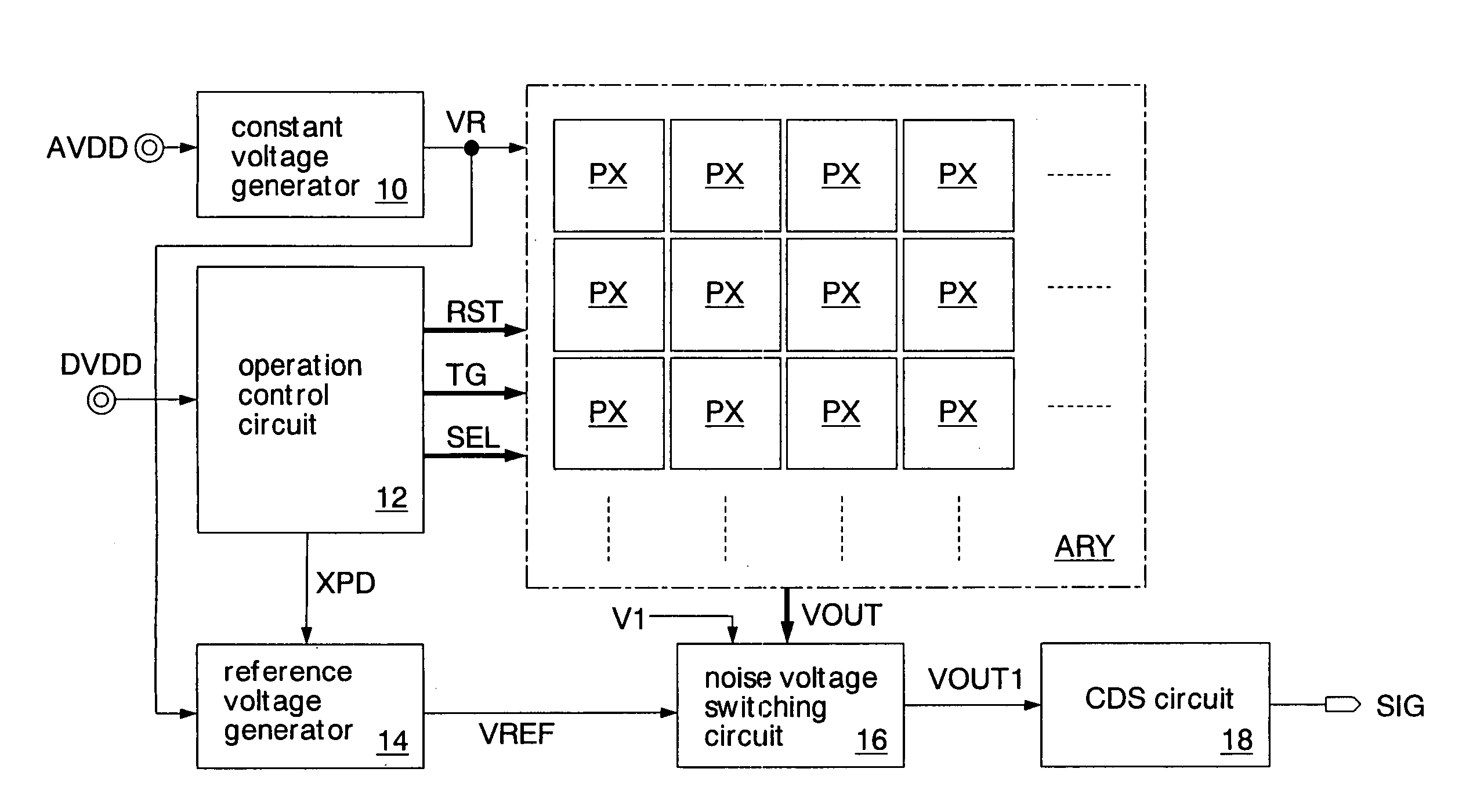
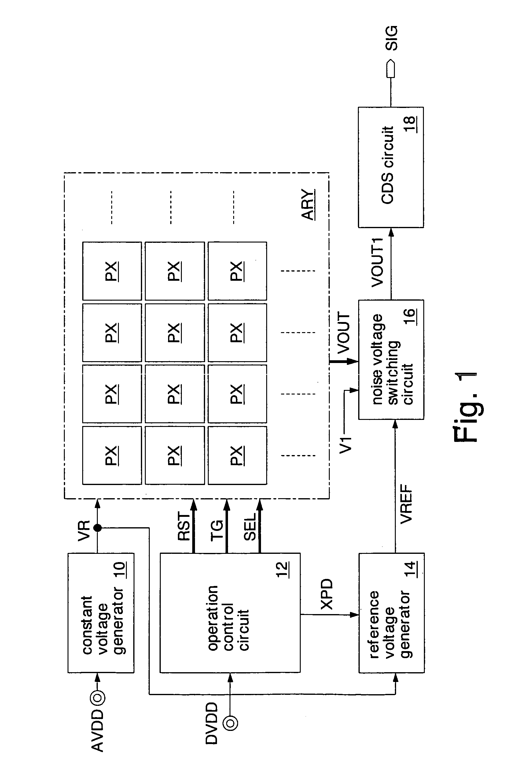
[0032]FIG. 1 shows an imaging device according to the present invention. This imaging device is formed as a CMOS image sensor chip on a silicon substrate using CMOS technology. The imaging device includes a constant voltage generator 10, an operation control circuit 12, a reference voltage generator 14, a noise voltage switching circuit 16, a correlated double sampling circuit (CDS circuit) 18, and a pixel array ARY.

[0033] The constant voltage generator 10 generates an internal voltage VR which is constant at all times, according to a power supply voltage AVDD. The power supply voltage AVDD is the power supply voltage for analog circuits. A power supply voltage DVDD for digital circuits may be supplied to the constant voltage generator 10. The internal voltage VR is the voltage lower than the power supply voltage AVDD, and is kept constant at all times irrespective of the change in the power supply voltage AVDD and the change in temperature. The operation control circuit 12 controls...

fourth embodiment

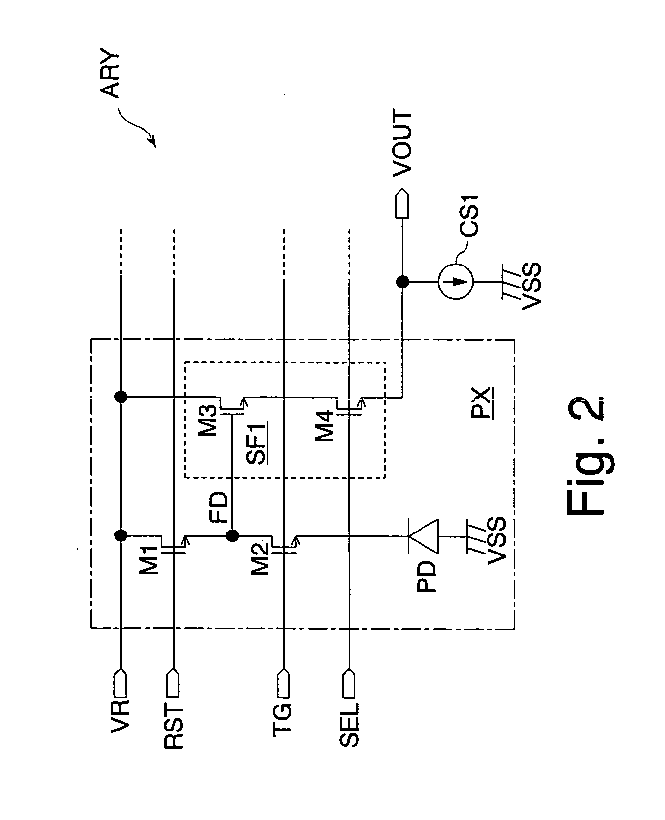
[0064]FIG. 9 shows the details of a pixel array ARY according to the The pixel array ARY includes a plurality of pixels PX arranged in a matrix state. Dummy pixels DPX formed in a dummy region DMY positioned on an outermost side of the pixel array ARY are not used for photoelectric conversion. The dummy pixels DPX are formed to form the inner pixels PX to have the ideal shape. On both right and left sides of the drawing, source follower areas SFA are formed inside the dummy region DMY. The source follower circuits SF3 shown in FIG. 8 are formed by using the source follower circuits SF1 which are formed in the pixels PX in the source follower areas SFA. Especially, the source follower circuits SF3 of this embodiment are formed by using the pixels PX which are shown in half-tone dot meshing and are positioned diagonally in the pixel array ARY.

[0065] Generally, in semiconductor devices, electric characteristics of elements are slightly different corresponding to the positions where th...

second embodiment

[0068] Incidentally, the above-described first and second embodiment have dealt with the case where the gate widths of the transistors M5 and M6 of the source follower circuit SF2 are designed to be twice as large as the gate widths of the transistors M3 and M4 of the source follower circuit SF1. However, the present invention is not limited to such embodiments. For example, the transistors M5 and M6 may be designed to have the identical size with the transistors M3 and M4. In this case, the source follower circuit SF2 may be constituted by using the source follower circuit SF1 of the pixel PX formed in the dummy region in the pixel array ARY or the like. By forming the source follower circuit SF2 inside the pixel array ARY, it is possible to equalize the electric characteristics of the source follower circuits SF1 and SF2 without fail.

[0069] The above-described fourth embodiment has dealt with the case where a pair of the source follower circuits SF3 are formed using the pixels PX ...


PUM


Abstract

A second source follower circuit of a reference voltage generator includes a transistor having the same characteristics as a first source follower circuit of a pixel. Accordingly, the second source follower circuit can generate a second reference voltage according to the change in characteristics of the first source follower circuit. A noise voltage switching circuit outputs a first voltage as a noise voltage to a pixel signal generator when the noise voltage is equal to or lower than the second reference voltage. In a reset state, the noise voltage and the second reference voltage always have a predetermined voltage difference. Therefore, deterioration in image quality can be prevented even when capturing a subject having high brightness. Since a trimming circuit or the like selecting any one of a plurality of reference voltages according to characteristics of a formed transistor becomes unnecessary, the cost of an imaging device can be reduced.

Description

CROSS-REFERENCE TO RELATED APPLICATIONS [0001] This application is based upon and claims the benefit of priority from Japanese Patent Application No. 2005-027771, filed on Feb. 3, 2005, the entire contents of which are incorporated herein by reference. BACKGROUND OF THE INVENTION [0002] 1. Field of the Invention [0003] The present invention relates to an imaging device including a photoelectric conversion element. More particularly, this invention relates to the technology of improving the quality of a captured image when capturing a subject having high brightness. [0004] 2. Description of the Related Art [0005] An imaging device such as a CMOS image sensor reads noise data (noise voltage) at respective photoelectric conversion elements during a reset period. For example, a correlated double sampling circuit (hereinafter also referred to as a CDS circuit) of the imaging device subtracts the noise data from pixel data which includes the read noise data, to thereby generate true pixel...

Claims


Application Information

Patent Timeline
Patent Type & Authority Applications(United States)
IPC IPC(8): H04N5/217H04N5/335H04N5/357H04N5/363H04N5/374
CPCH03F3/087H04N5/3575H04N5/3598H04N5/363H04N25/627H04N25/616H04N25/65H04N25/60H04N25/76
Inventor HIGUCHI, TSUYOSHIFUNAKOSHI, JUNYAMAGATA, SEIJIMIZUGUCHI, TOSHITAKAYAMAMOTO, KATSUYOSHI
Owner SOCIONEXT INC
Why Eureka
Try Eureka