Light emitting element and light emitting device

a technology of light emitting elements and light emitting devices, which is applied in the field of light, can solve the problems of easy short circuit between the upper electrode and the lower electrode, the insufficient means disclosed in the patent document 1, and the insufficient means to prolong the lifetime of the light emitting element, etc., and achieves the suppression of the increase in driving voltage, prolonging the lifetime, and low activation energy of electrical conductivity

Active Publication Date: 2006-08-17
SEMICON ENERGY LAB CO LTD
View PDF35 Cites 49 Cited by
  • Summary
  • Abstract
  • Description
  • Claims
  • Application Information

AI Technical Summary

Benefits of technology

[0023] Providing a layer having low activation energy of electrical conductivity in a light emitting element of the present invention makes it possible to suppress increase in driving voltage. Moreover, a light emitting element having longer lifetime can be provided.
[0024] Since the increase in driving voltage can be suppressed in the

Problems solved by technology

However, only the means disclosed in the patent document 1 is not sufficient to prolong lifetime of a light emitting element.
In addition, since a light emitting element is generally formed using a thin organic film, for example, with a thickness of about 0

Method used


Image

  • Light emitting element and light emitting device
  • Light emitting element and light emitting device
  • Light emitting element and light emitting device

Examples


embodiment mode 1

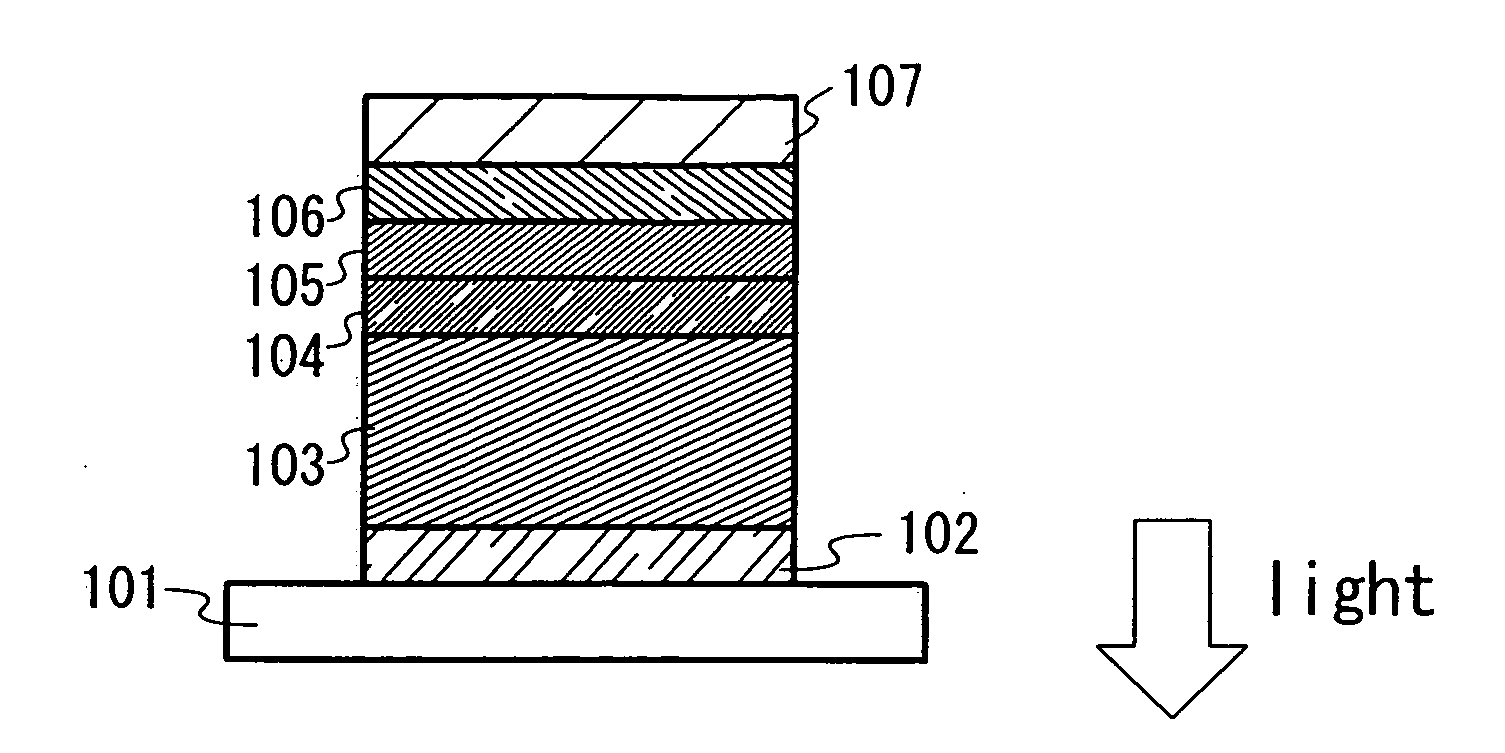
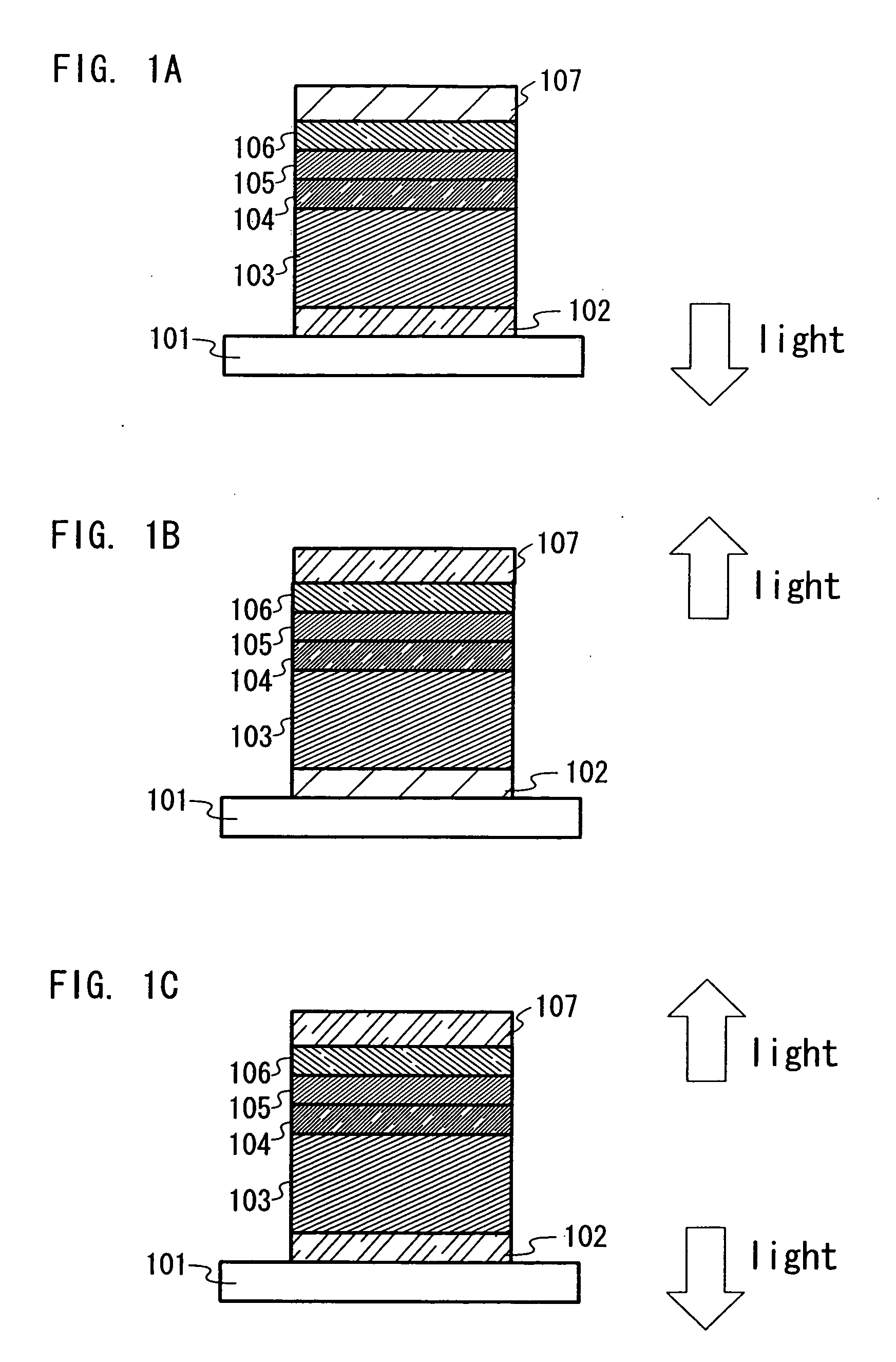
[0052] A light emitting element of the present invention includes a plurality of layers between a pair of electrodes. The plurality of layers are laminated by combining layers made from a substance having a strong carrier injecting property and a substance having a strong carrier transporting property such that a light emitting region is formed away from the electrodes, or, carriers (supports) are recombined at a portion away from the electrodes.

[0053] One mode of the light emitting element of the present invention will be described with reference to FIG. 1A.

[0054] In this embodiment mode, the light emitting element includes a first electrode 102, a laminated body formed by laminating a first layer 103, a second layer 104, a third layer 105 and a fourth layer 106, over the first electrode 102 in this order, and a second electrode 107 provided on the fourth layer 106. In this embodiment mode, the first electrode 102 serves as an anode and the second electrode 107 serves as a cathod...

embodiment mode 2

[0079] In this embodiment mode, a layer having low activation energy of electrical conductivity shown in Embodiment Mode 1 (i.e., a layer containing both an organic material and an inorganic material, and whose activation energy of electrical conductivity is 0.01 eV or more and less than 0.30 eV, preferably, 0.01 eV or more and less than 0.26 eV, and more preferably, 0.01 eV or more and less than 0.20 eV) will be described in more detail.

[0080] A case where a layer containing both an organic material and an inorganic material, does not have an absorption peak in a visible light region, will be described in this embodiment mode. Specifically, a layer containing DNTPD and molybdenum oxide, which does not have an absorption peak in a visible light region, will be described in this embodiment mode. FIG. 11 shows an absorption spectrum of a layer containing DNTPD and molybdenum oxide, which is formed by co-evaporation such that a weight ratio between DNTPD and molybdenum oxide is 1:1. A...

embodiment mode 3

[0098] A case where a layer containing both an organic material and an inorganic material has an absorption peak in a visible light region, which is different from Embodiment Mode 2, will be described in this embodiment mode. In this embodiment mode, a layer containing BSPB and molybdenum oxide, which has an absorption peak in the visible light region, will be described. FIG. 12 shows an absorption spectrum of a layer, which is formed by co-evaporation of BSPB and molybdenum oxide such that a weight ratio between BSPB and molybdenum oxide is 1:1. According to FIG. 12, it is known that the layer containing BSPB and molybdenum oxide has an absorption peak in the visible light region. In addition to BSPB, a layer containing an organic material such as TPD, α-NPD, DFLDPBi and BBPB, and molybdenum oxide has an absorption peak in the visible light region.

[0099] A film with a thickness of 110 nm was formed using ITO over a first glass substrate to form an anode having an area of 4 mm2. Th...


PUM


Abstract

The present invention provides a light emitting element whose driving voltage is low, and a light emitting element having longer lifetime. Moreover, the invention provides a light emitting element with high manufacturing yield. A light emitting element has a layer containing an organic material and an inorganic material, wherein activation energy of electrical conductivity of the layer containing the organic material and the inorganic material, is 0.01 eV or more and less than 0.30 eV. Preferably, the activation energy of electrical conductivity of the layer containing the organic material and the inorganic material, is 0.01 eV or more and less than 0.26 eV. More preferably, the activation energy of the electrical conductivity of the layer containing the organic material and the inorganic material, is 0.01 eV or more and less than 0.20 eV.

Description

BACKGROUND OF THE INVENTION [0001] 1. Field of the Invention [0002] The present invention relates to a light emitting element having a structure in which a plurality of layers are interposed between a pair of electrodes. Moreover, the present invention relates to a light emitting device having the light emitting element. [0003] 2. Description of the Related Art [0004] A light emitting device utilizing light emitted from an electroluminescence element (a light emitting element) has been attracting attention as a display device or a lighting device. [0005] As a light emitting element used for a light emitting device, a light emitting element in which a layer containing a light emitting compound is interposed between a pair of electrodes, is well known. [0006] In such a light emitting element, one of the pair of electrodes serves as an anode and the other electrode serves as a cathode. Holes injected from the anode and electrons injected from the cathode are recombined to form excited ...

Claims


Application Information

Patent Timeline
IPC IPC(8): H01L29/08
CPCH01L27/3244H01L51/0059H01L51/006H01L51/5012H01L2251/5315H01L2251/5323H10K59/12H10K85/633H10K85/631H10K50/11H10K2102/3026H10K2102/3031
Inventor SAKATA, JUNICHIROKAWAKAMI, TAKAHIROIKEDA, HISAO
Owner SEMICON ENERGY LAB CO LTD
Why Eureka
Try Eureka