Method and apparatus for measuring wafer thickness

a technology of wafer thickness and measurement method, applied in the direction of measuring device, using optical means, instruments, etc., can solve the problems that prior art systems with relatively large optical focus spots are not suitable for bump wafer analysis, and achieve the effects of small focused spots, high degree of resolution, and easy measuremen

Active Publication Date: 2006-08-17
CHAPMAN INSTR
View PDF7 Cites 10 Cited by
  • Summary
  • Abstract
  • Description
  • Claims
  • Application Information

AI Technical Summary

Benefits of technology

[0014] An important advantage of the present system is that a very small focused spot may be used, on the order of about 1 μm. When means are provided to translate the test object orthogonal to the beams, the wafer thickness can be readily measured to a very high degree of resolution in the presence of surface features. This can be very useful, for example, in characterizing so-called “bump wafers” which have small bumps all over the wafer for interconnect. This is a relatively new concept and is bein

Problems solved by technology

Prior art systems having relatively large optical f

Method used


Image

  • Method and apparatus for measuring wafer thickness
  • Method and apparatus for measuring wafer thickness
  • Method and apparatus for measuring wafer thickness

Examples


Embodiment Construction

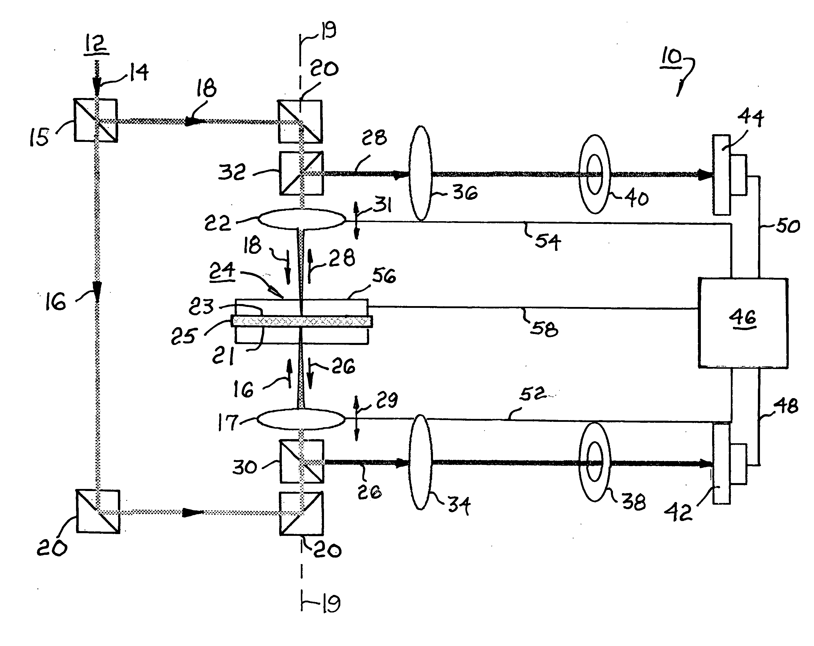
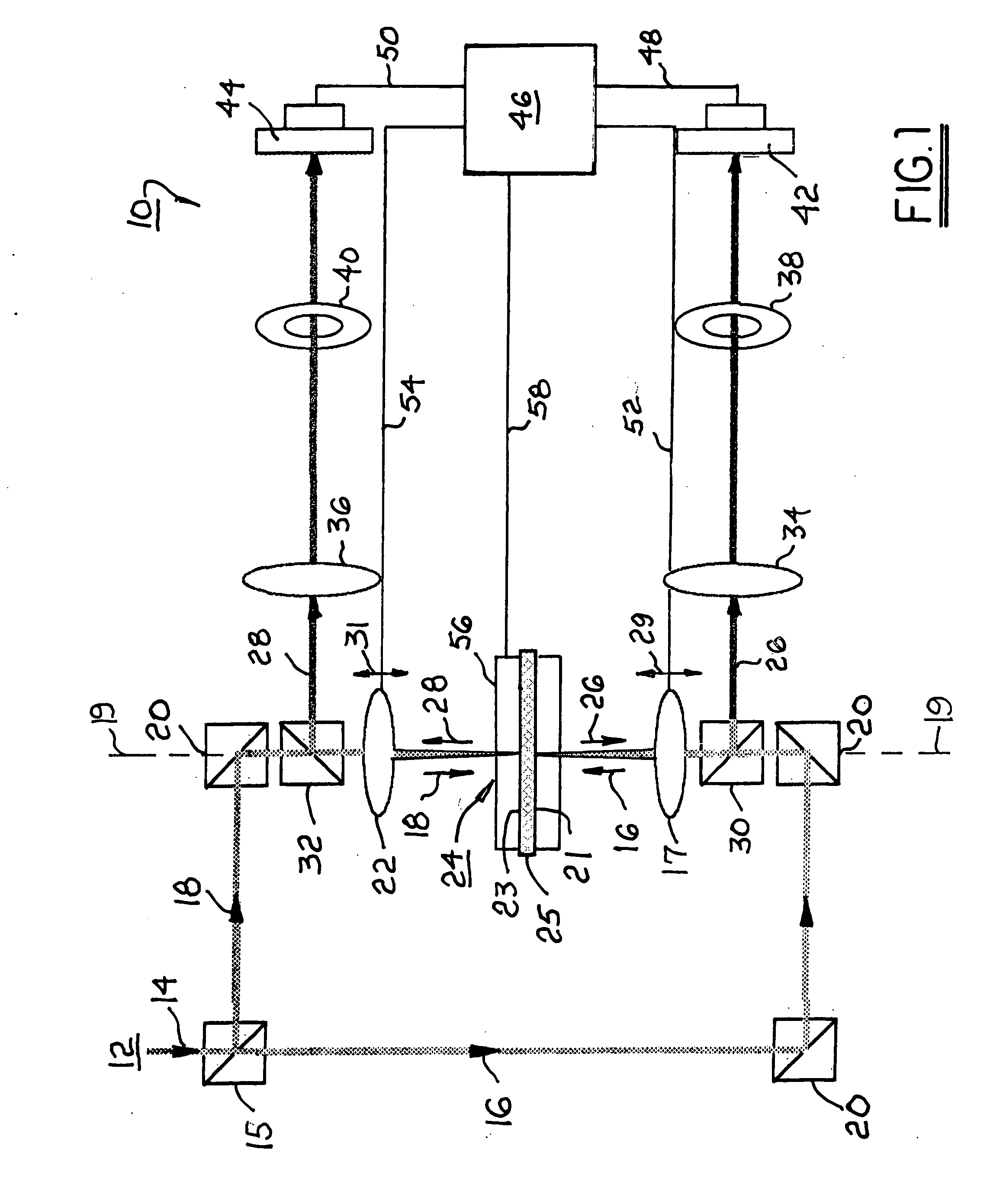
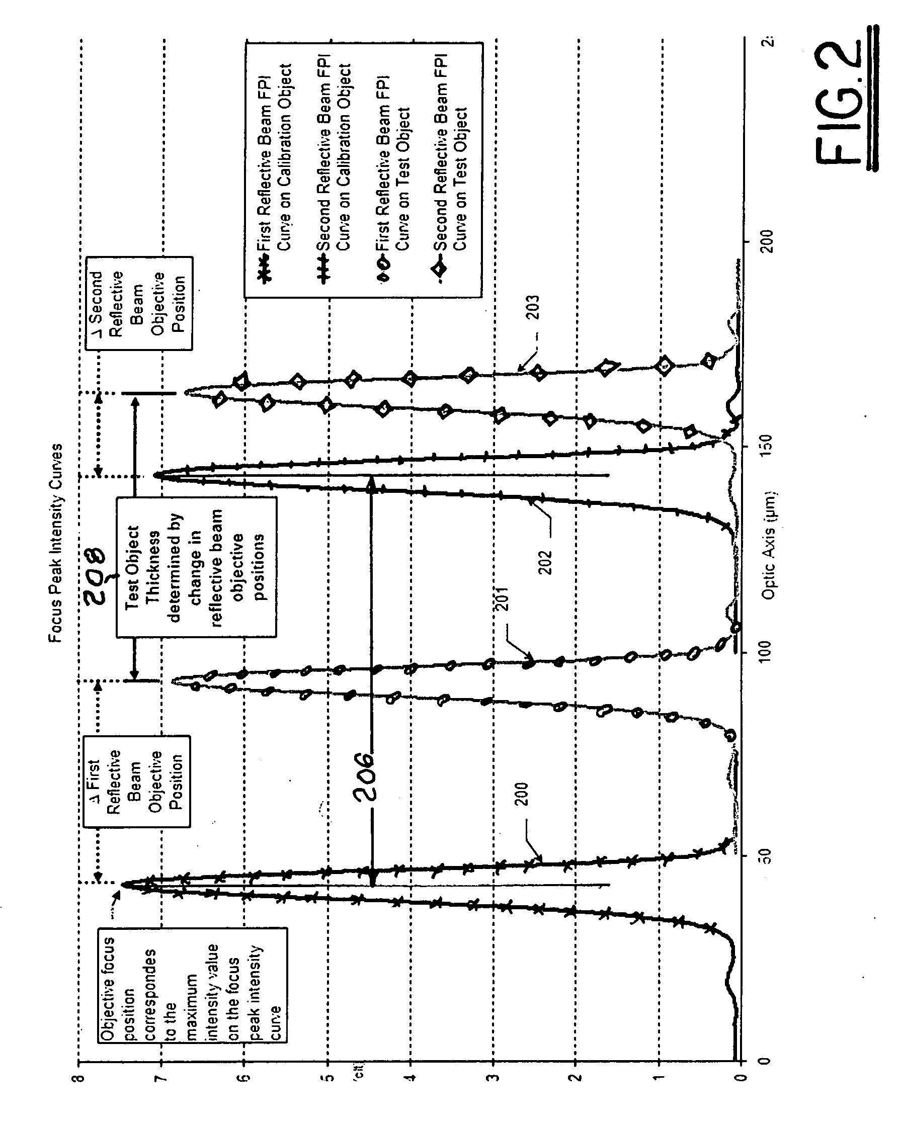
[0018] Referring to FIG. 1, a non-contact thickness measurement system 10 in accordance with the invention includes a light-generating source 12 capable of producing a master beam 14. Beam 14 may be incoherent but preferably is a laser beam. A first beam splitter 15 divides master beam 14 into first and second input beams 16,18 which preferably are substantially identical in intensity. Angled mirrors 20 turn beams 16,18 such that they are in opposition along an optic axis 19. First and second focussing means 17,22 are provided for focussing input beams 16,18 independently in a space 24 between focussing means 17 and 22. Focussing means 17,22 are independently movable 29,31 along optic axis 19 to vary the axial positions of their respective focal points within space 24. When reflective surfaces 21,23 of a test object 25 are placed in space 24, first and second reflective beams 26,28 from surfaces 21,23 are turned by half-mirrors 30,32, respectively, to direct reflective beams 26,28 t...


PUM


Abstract

A system for non-contact measurement of thickness of a test object. A laser beam is split into two identical directly opposed input beams. A calibration object of known thickness causes beams to be reflected from sides of the test object. Each reflected beam passes through sensing means including a pinhole aperture and a photodiode sensor. Maximum sensor output defines first and second focal points a known distance apart. The calibration object is removed, and the test object is inserted into the path of the input beams, creating focus position intensity curves for the reflected beams. By determining the deviation, at maximum photodiode output, of the positions of the test object reflecting surfaces from the positions of the calibration object surfaces, the test object thickness can be readily and accurately determined.

Description

[0001] The present application is a Continuation-In-Part of a pending U.S. patent application Ser. No. 10 / 946,450, filed Sep. 21, 2004.TECHNICAL FIELD [0002] The present invention relates to means for measuring thickness of objects; more particularly, to method and apparatus for non-contact measurement of thickness; and most particularly, to method and apparatus for non-contact measuring the thickness of a planar reflective object such as a silicon wafer or a flat panel display. BACKGROUND OF THE INVENTION [0003] Silicon wafers are important elements of the semiconductor industry. Such wafers typically are sawn from artificially-grown silicon crystals and require one or more surface finishing or conditioning operations, each of which causes progressive thinning of a wafer. [0004] The semiconductor industry is moving toward thinner wafers, especially important for smart cards, flash memory, and other products requiring thin packaging. One of the challenges for thin wafer manufacturin...

Claims


Application Information

Patent Timeline
IPC IPC(8): G01B11/28
CPCG01B11/06
Inventor BRISTOW, THOMAS C.WANG, SHU W.STEPHAN, JOHN E.
Owner CHAPMAN INSTR
Why Eureka
Try Eureka