Overvoltage-protected light-emitting semiconductor device

a technology of overvoltage protection and semiconductor devices, which is applied in the direction of emergency protective arrangements for limiting excess voltage/current, semiconductor/solid-state device details, and arrangements responsive to excess voltage, etc., can solve the problems of increasing the size of the complete device, unnecessarily bulky in size, and difficult to set the forward voltage of the protector diode as desired or required, etc. , to achieve the effect of less expensive construction, simple structure and less bulky

Active Publication Date: 2006-08-17
SANKEN ELECTRIC CO LTD
View PDF2 Cites 58 Cited by
  • Summary
  • Abstract
  • Description
  • Claims
  • Application Information

AI Technical Summary

Benefits of technology

[0011] The present invention has it as an object to combine a light-emitting semiconductor device and an overvoltage prot...

Problems solved by technology

First of all, it is unnecessarily bulky in size as an inevitable result of the side-by-side arrangement of the LED and the protector diode on the sapphire substrate.
Another drawback arises from the epitaxial growth of the protector diode at the same time with that of the LED according to Japanese Unexamined Patent Publication No. 10-65215, supra.
The thickness of the protector diode is therefore subject to that of the LED, making it difficult to set the forward voltage of the protector diode as desired or required.
This risk is p...

Method used


Image

  • Overvoltage-protected light-emitting semiconductor device
  • Overvoltage-protected light-emitting semiconductor device
  • Overvoltage-protected light-emitting semiconductor device

Examples


embodiment

of FIG. 5

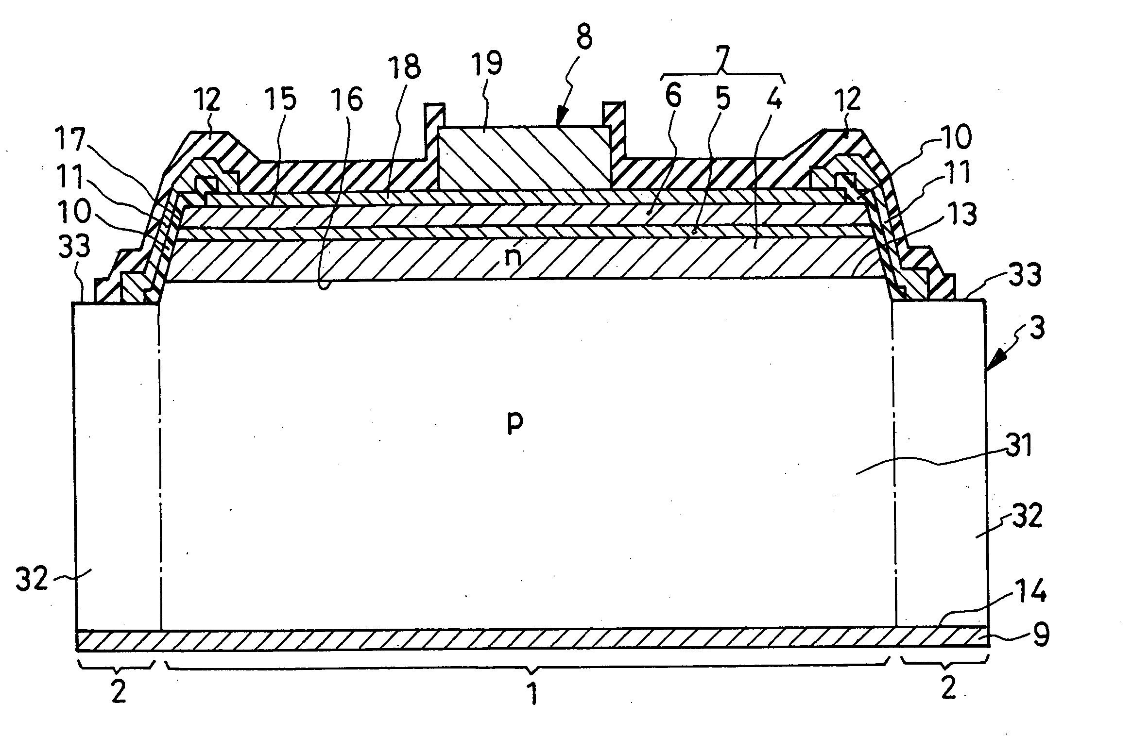
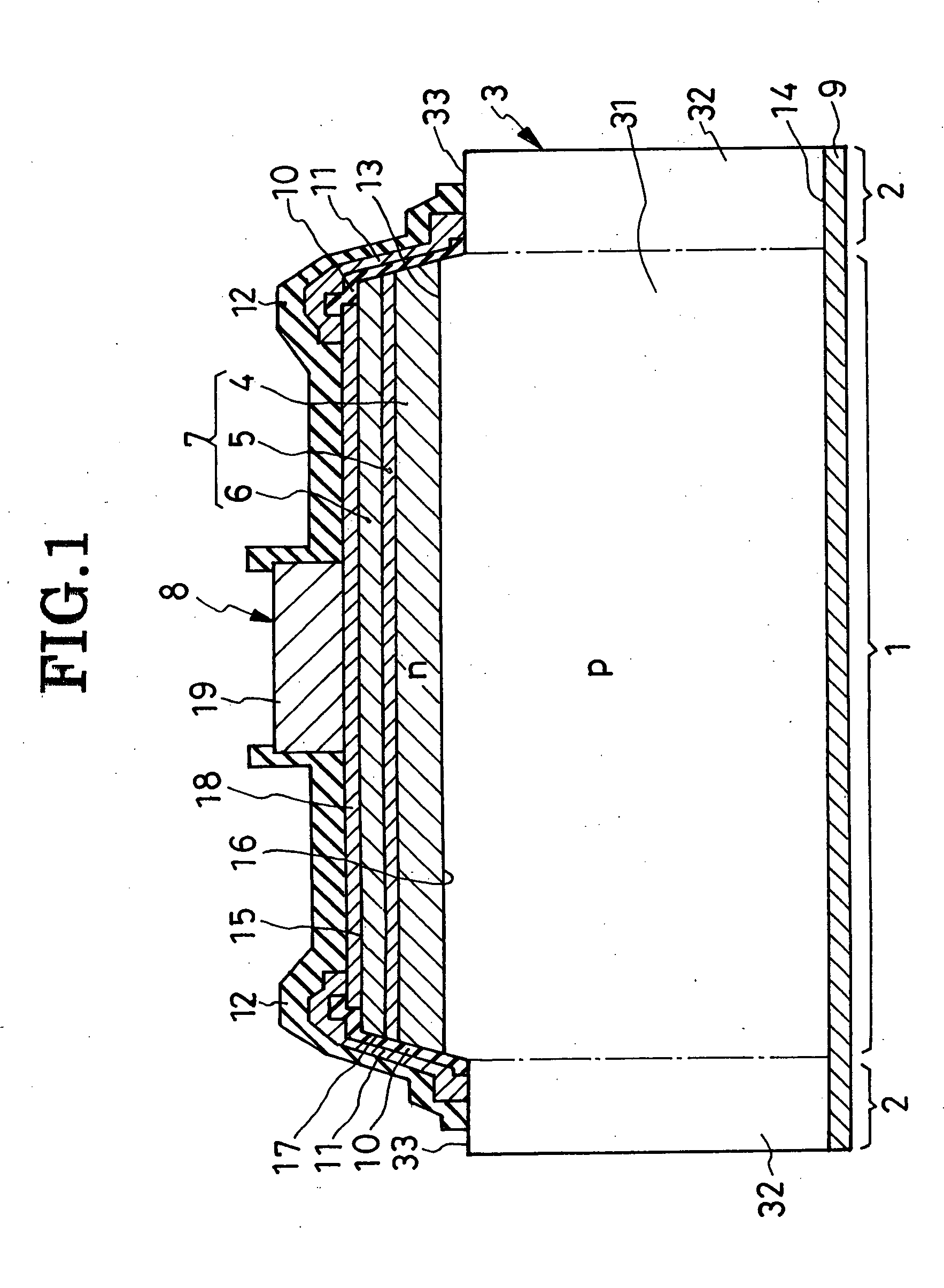
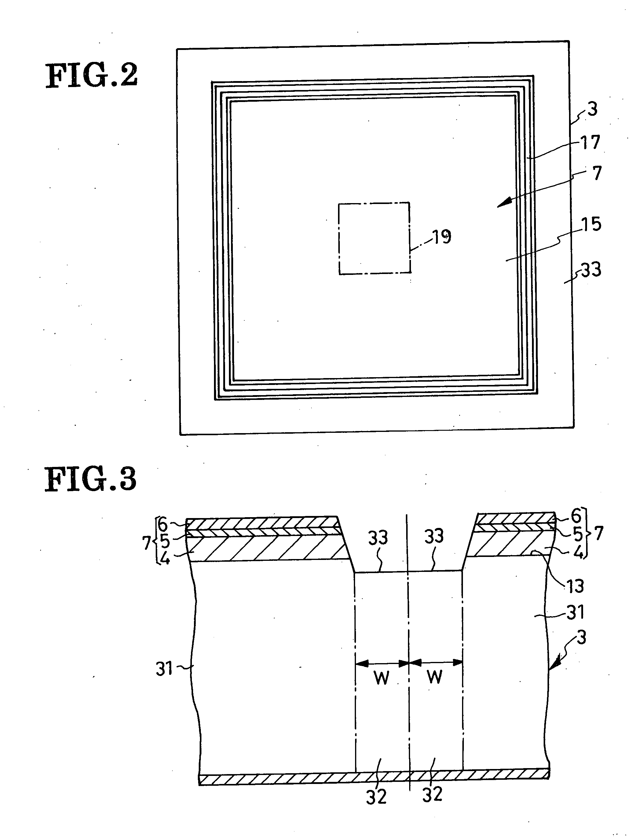
[0080] The second preferred form of overvoltage-protected LED shown in FIG. 5 differs from the FIG. 1 embodiment only in its overvoltage protector section 2a. The modified protector section 2a differs in turn from its FIG. 1 counterpart only in the absence of the insulating film 10.

[0081] As a result of the absence of the insulating film 10, the n-type semiconductor film 11 of the modified protector section 2a is directly held against the slanting side surfaces 17 of the light-generating semiconductor region 7. The n-type semiconductor film 11 may therefore be made from a material that is greater in bandgap than that of the active layer 5, preferably than those of all the constituent layers 4-6 of the light-generating semiconductor region 7. Possible current leakage from semiconductor film 11 to light-generating semiconductor region 7, or vice versa, will then be practically negligible. The other details of construction and operation as well as the resulting advantages are...


PUM


Abstract

An LED incorporating an overvoltage protector with a minimum of space requirement. The LED itself comprises a p-type semiconductor substrate, a light-generating semiconductor region grown epitaxially thereon, a first electrode on the light-generating semiconductor region, and a second electrode on the underside of the substrate. The standard method of LED fabrication is such that the substrate is notionally divisible into a main portion in register with the overlying light-generating semiconductor region and, surrounding the main portion, a tubular marginal portion needed for dicing the wafer into individual squares or dice. The overvoltage protector comprises an n-type semiconductor film formed on the marginal portion of the substrate and held against the side surfaces of the light-generating semiconductor region via an insulating film. Creating a pn junction with the marginal portion of the p-type substrate, the n-type semiconductor film provides an overvoltage protector diode which is electrically connected reversely in parallel with the LED. Various other embodiments are disclosed.

Description

CROSS REFERENCE TO RELATED APPLICATIONS [0001] This application claims priority to Japanese Patent Application No. 2005-039649, filed Feb. 16, 2005. BACKGROUND OF THE INVENTION [0002] This invention relates to light-emitting semiconductor devices, or light-emitting diodes (LEDs) according to common parlance, and more specifically to such devices integrally incorporating an overvoltage protector. [0003] Currently attracting the attention of the specialists in the light-emitting semiconductor art are the nitrides capable of generating light in the wavelength range of 365 to 550 nanometers. The devices employing this class of nitride semiconductors, as heretofore made, were mostly capable of resisting electrostatic breakdown only up to 100 volts or so. Attempts have been made to make the devices more immune to electrostatic breakdown. Japanese Unexamined Patent Publication Nos. 10-65215 and 10-200159 are examples. They teach to build an overvoltage protector, which takes the form of a ...

Claims


Application Information

Patent Timeline
IPC IPC(8): H02H9/04H01L33/32H01L21/822H01L27/04H01L27/15H01L33/42H01L33/44
CPCH01L27/15H01L23/62H01L2924/0002H01L2924/00
Inventor SATO, JUNJITAZIMA, MIKIOMOKU, TETSUJINIWA, AREIKAMII, YASUHIRO
Owner SANKEN ELECTRIC CO LTD
Why Eureka
Try Eureka