Method and apparatus for generating synchronization signals for synchronizing multiple chips in a system
a technology of synchronization signals and chips, applied in the direction of generating/distributing signals, synchronization signal speed/phase control, digital transmission, etc., can solve the problem of insufficient time, and achieve the effect of reducing timing uncertainty in cross-chip communication systems
- Summary
- Abstract
- Description
- Claims
- Application Information
AI Technical Summary
Benefits of technology
Problems solved by technology
Method used
Image
Examples
embodiment i
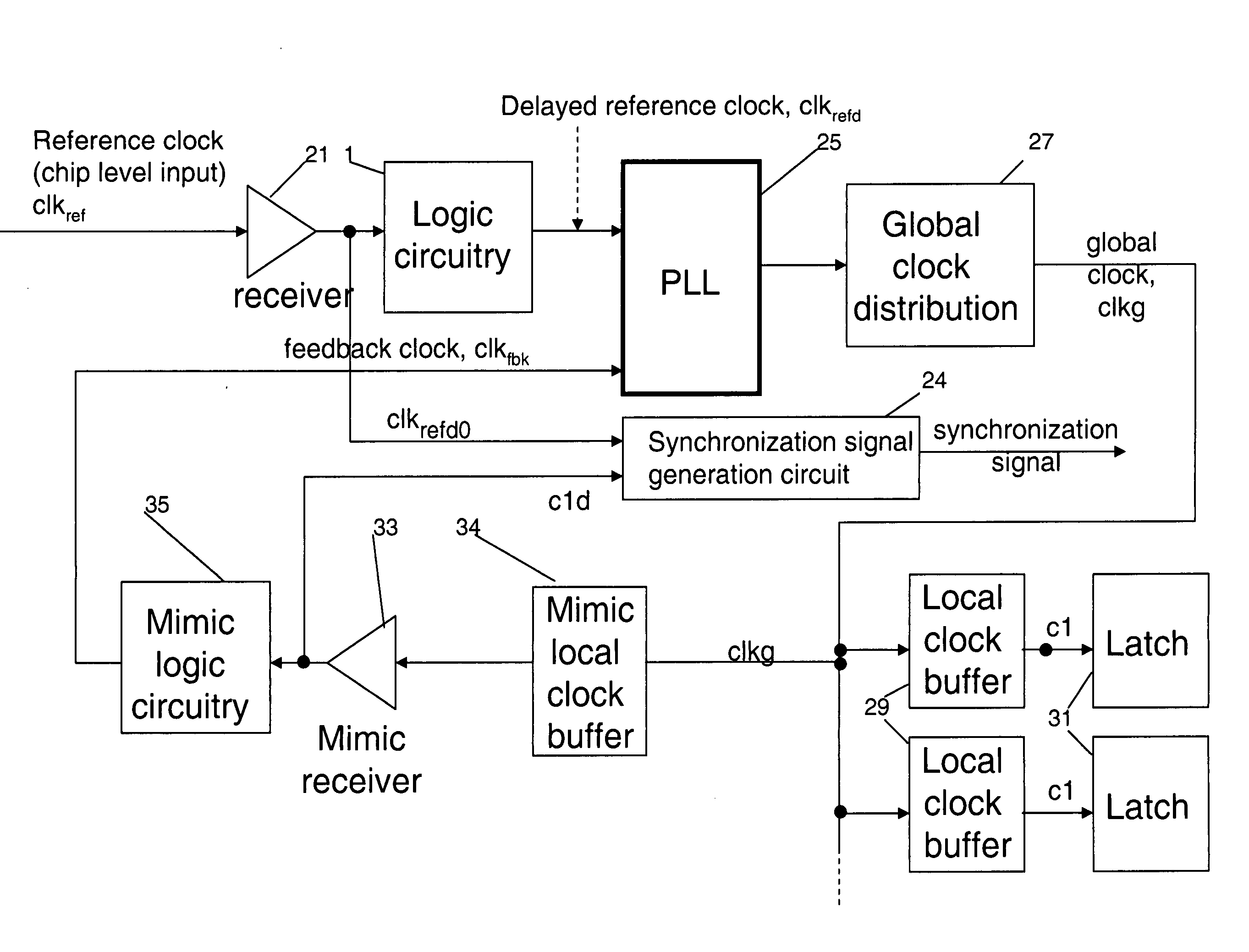
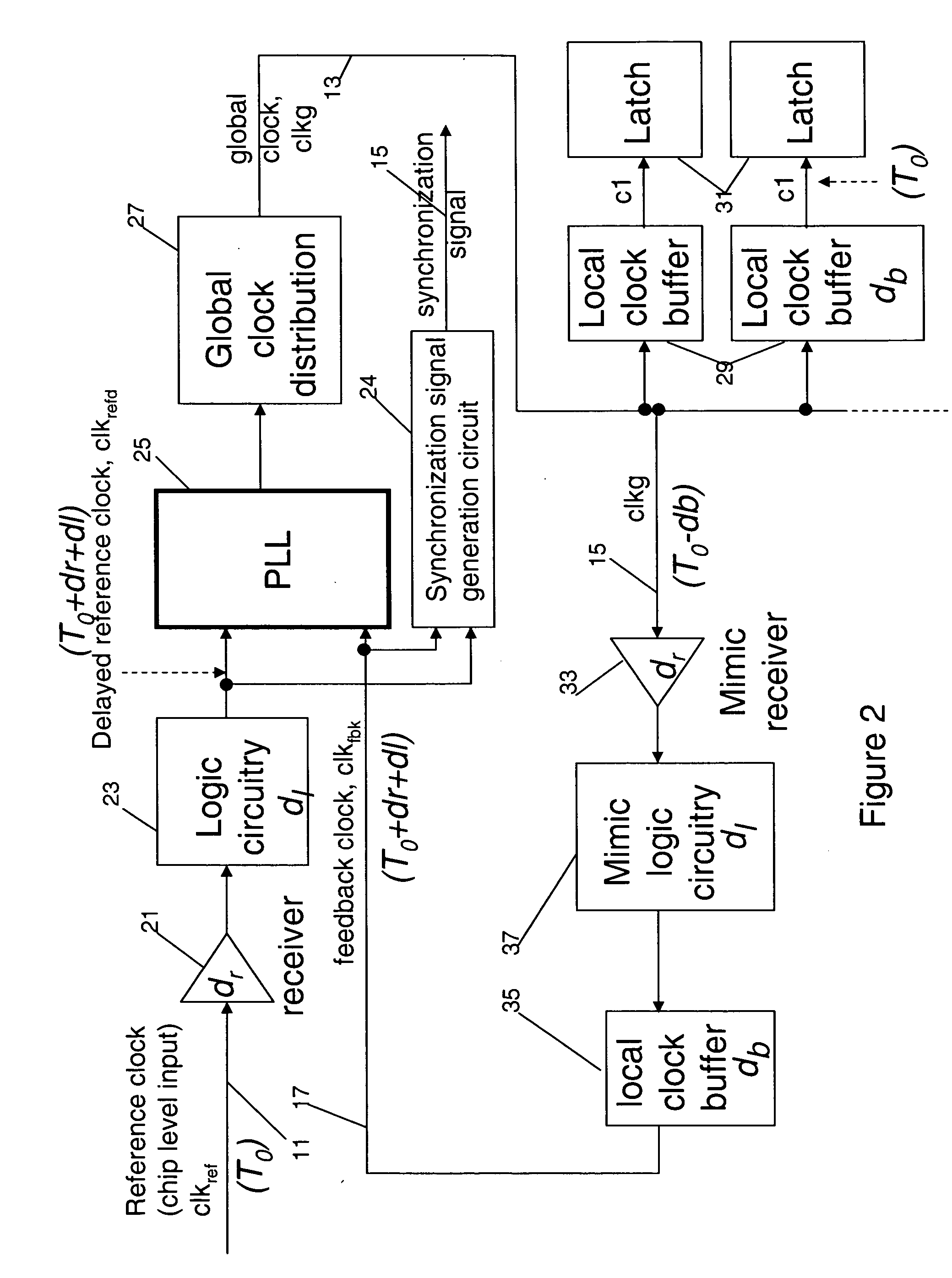
[0032] When the delay of the mimic circuitry is around 1 clkg cycle but less than 1.5 clkg cycles, the first latch to receive the synchronization signal is placed close to the synchronization signal generation circuit. The feedback is inverted and used to clock latch 1 as shown in FIG. 4. The output from the synchronization signal generation circuit is still launched with feedback clock. Effectively, this scheme borrows 0.5 clkg cycle from the next path between latch 1 and latch 2, so latch 1 to latch 2 becomes a half-cycle path. In physical design, latch 2 also need to be placed close to latch one to allow the half cycle path.
[0033] Other variations to this scheme include using inverted feedback clock to clock the synchronization generation circuit as shown in FIG. 7a. By doing so, the path between the launching latches and latch 1 receive one full cycle for signal transfer. This allow additional combinational logic to be added to the path for other functions.
embodiment ii
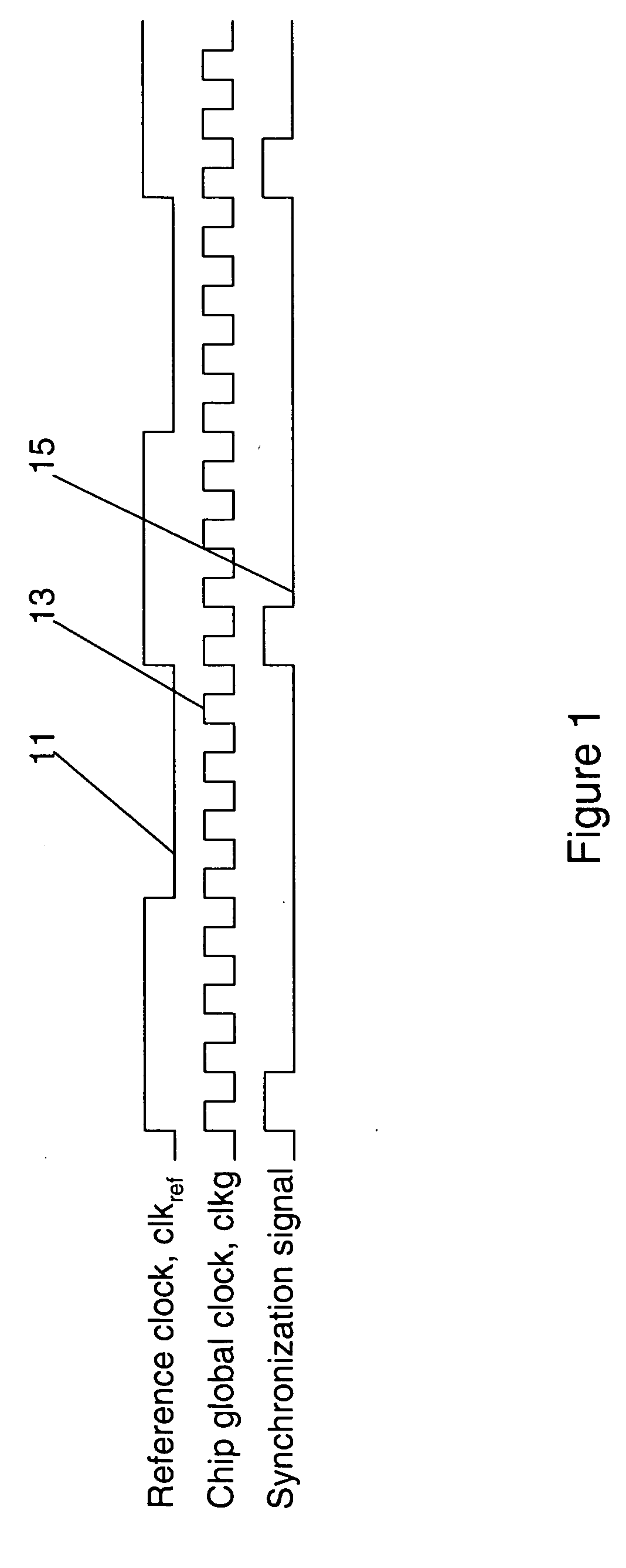
[0034] When, td is more than 1.5 times of the minimum global clock cycle time, even the approach used by embodiment I is not adequate to receive the synchronization signal at the second latch, clocked by clkg, without uncertainty. When the chip runs at slower frequency than the maximum frequency, the cycle relative to clkg that the synchronization signal is latched at latch 2 may become uncertain if the mimic circuitry delay, td, is close to the integral multiple of slowed down clkg cycle time as shown in FIG. 6. It is critical that the method used will operate at the maximum frequency and any frequency that is slower than the design frequency. In today's modern processors, the frequency of operation is often slowed down to save power, to prevent over heating, for speed sorting, or for testing. The system must continue to function under these slower frequencies.
[0035] To make the design frequency independent, we'll need to generate the synchronization signal with two other clock so...
PUM
 Abstract
Description
Claims
Application Information


