Nitrogen rich barrier layers and methods of fabrication thereof

a technology of barrier layer and nitrogen rich, which is applied in the direction of semiconductor devices, basic electric elements, electrical equipment, etc., can solve the problems of reducing the electrical resistance of the barrier layer, and achieve the effects of improving the copper diffusion barrier properties, reducing electrical resistance, and increasing oxidation resistan

Active Publication Date: 2006-08-17
INFINEON TECH AG
View PDF6 Cites 54 Cited by
  • Summary
  • Abstract
  • Description
  • Claims
  • Application Information

AI Technical Summary

Benefits of technology

[0011] Advantages of preferred embodiments of the present invention include providing improved barrier layers having a nitrogen rich region at the top surface thereof. The novel barrier layers described herein have im

Problems solved by technology

In some embodiments, only the surface of the barrier layers are nitri

Method used


Image

  • Nitrogen rich barrier layers and methods of fabrication thereof
  • Nitrogen rich barrier layers and methods of fabrication thereof
  • Nitrogen rich barrier layers and methods of fabrication thereof

Examples


Embodiment Construction

[0020] The making and using of the presently preferred embodiments are discussed in detail below. It should be appreciated, however, that the present invention provides many applicable inventive concepts that can be embodied in a wide variety of specific contexts. The specific embodiments discussed are merely illustrative of specific ways to make and use the invention, and do not limit the scope of the invention.

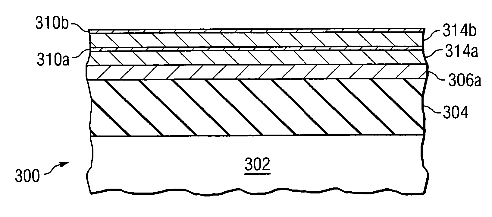
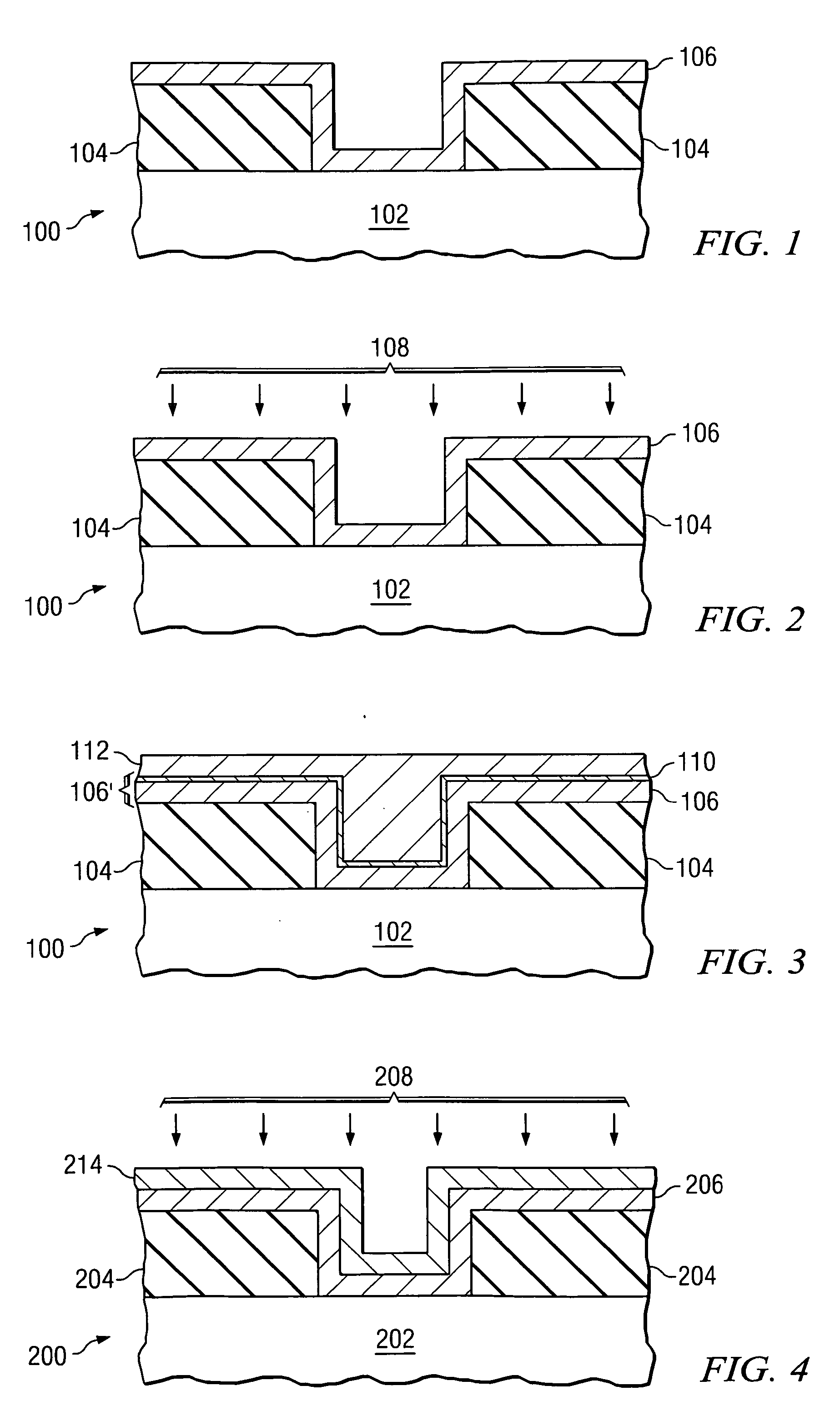
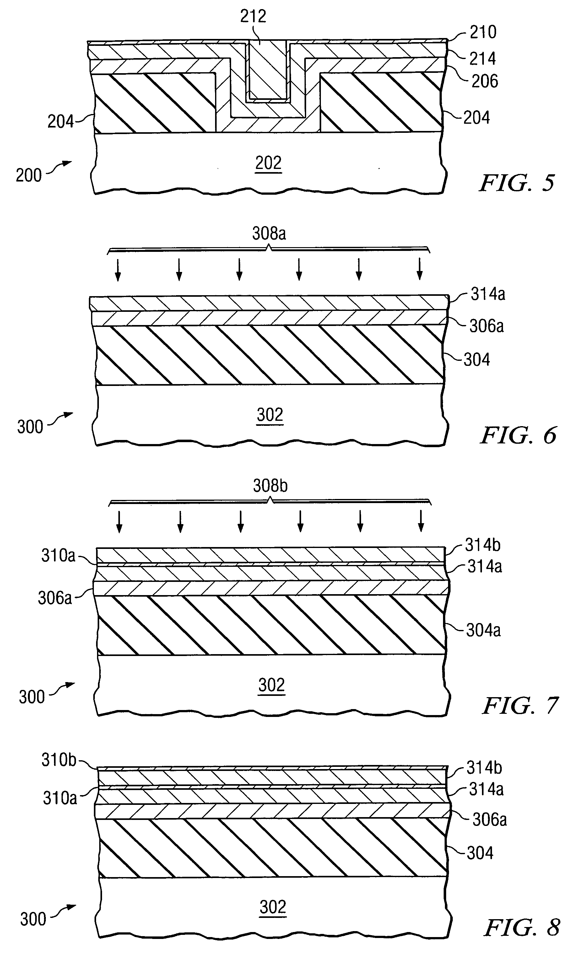
[0021] The present invention will be described with respect to preferred embodiments in a specific context, namely the formation of barrier layers on insulating material layers. The invention may also be applied, however, to the formation of barrier layers on other material layers, such as semiconductive materials or conductive materials, as examples.

[0022] Embodiments of the present invention achieve technical advantages by providing novel methods of forming barrier layers having improved properties, such as improved diffusion prevention and increased oxidation resistance...


PUM


Abstract

Methods of forming barrier layers and structures thereof are disclosed. A nitrogen rich region is formed at a top surface of a barrier layer by exposing the barrier layer to a nitridation treatment. The nitrogen rich region increases the oxidation resistance of the barrier layer. The barrier layers have improved diffusion barrier properties. A stack of barrier layers may be formed, with one or more of the barrier layers in the stack being exposed to a nitridation treatment.

Description

TECHNICAL FIELD [0001] The present invention relates generally to the fabrication of semiconductors, and more particularly to methods of forming barrier layers of semiconductor devices. BACKGROUND [0002] Semiconductor devices are used in a variety of electronic applications, such as computers, cellular phones, personal computing devices, and many other applications. Home, industrial, and automotive devices that in the past comprised only mechanical components now have electronic parts that require semiconductor devices, for example. [0003] Semiconductor devices are manufactured by depositing many different types of material layers over a semiconductor workpiece or wafer, and patterning the various material layers using lithography. The material layers typically comprise thin films of conductive, semiconductive, and insulating materials that are patterned and etched to form integrated circuits (IC's). There may be a plurality of transistors, memory devices, switches, conductive lines...

Claims


Application Information

Patent Timeline
IPC IPC(8): H01L21/44
CPCH01L21/76843H01L21/76846H01L21/76856H01L2221/1078
Inventor MOON, BUM KI
Owner INFINEON TECH AG
Why Eureka
Try Eureka