Vertical batch processing apparatus

a technology of batch processing and equipment, applied in the direction of vacuum evaporation coating, transportation and packaging, coatings, etc., can solve the problems of unfavorable fluorine on the wafer surface, low electrical characteristics of the semiconductor device, and inability to clarify the structure and material of the apparatus for forming ammonium silicofluoride, etc., to achieve high reliability

Inactive Publication Date: 2006-08-24
TOKYO ELECTRON LTD
View PDF6 Cites 248 Cited by
  • Summary
  • Abstract
  • Description
  • Claims
  • Application Information

AI Technical Summary

Benefits of technology

[0011] An object of the present invention is to provide a vertical batch processing apparatus and semiconductor processing system including the same, which can be used with high reliability to remove a semiconductor oxide film present on target objects, such as semiconductor wafers.

Problems solved by technology

The natural oxide film can cause semiconductor devices to have lower electrical characteristics or to be defective.
In this case, the wafer surface unfavorably suffers fluorine left thereon.
However, the structure and material of an apparatus for forming ammonium silicofluoride are not clarified.
In this case, however, the gases may be insufficiently activated.
In this case, the interior of the process chamber is exhausted from the bottom, and the gases may less uniformly flow in the process chamber.

Method used


Image

  • Vertical batch processing apparatus
  • Vertical batch processing apparatus
  • Vertical batch processing apparatus

Examples


first embodiment

[0055] [Semiconductor Processing System]

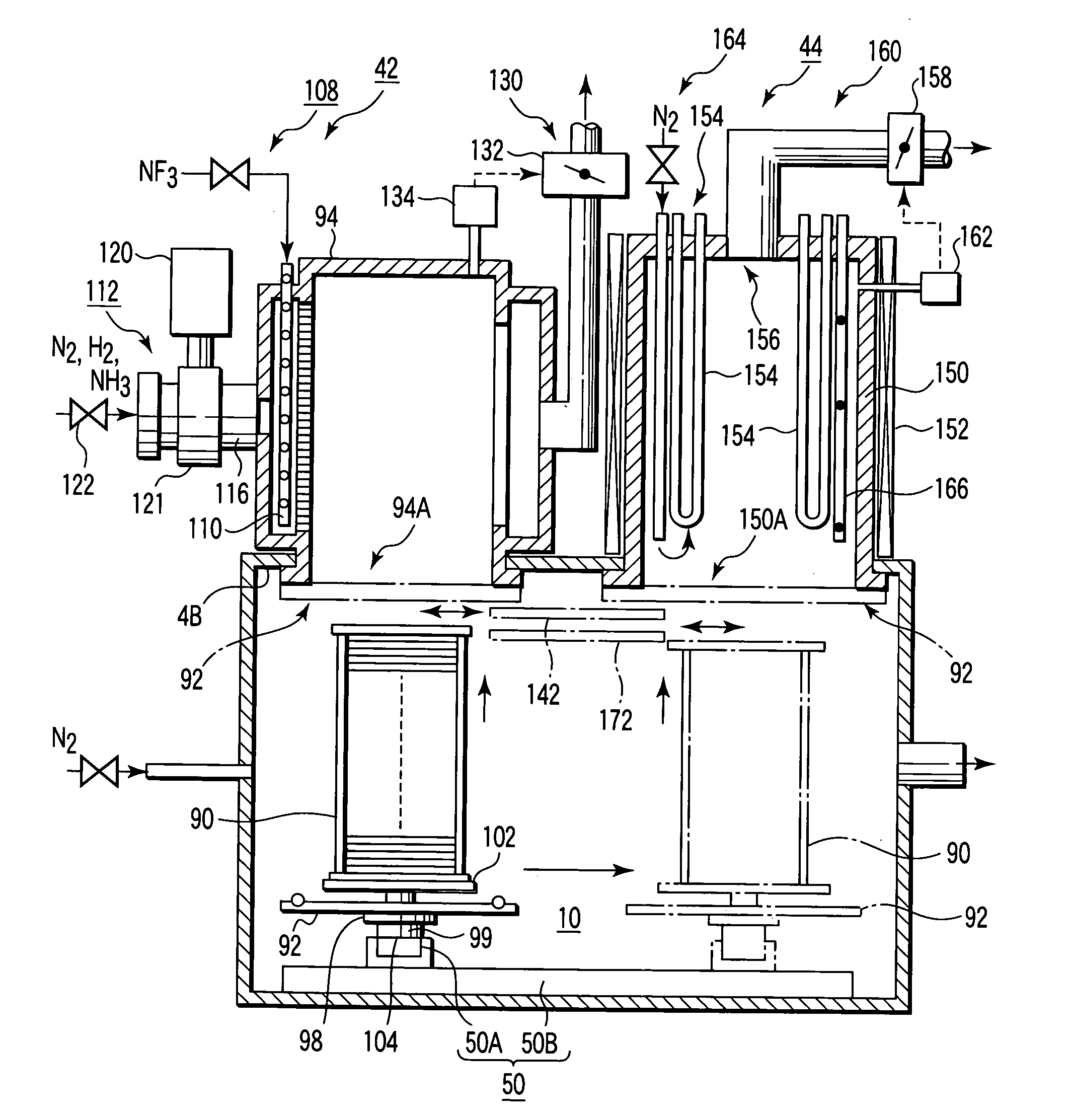
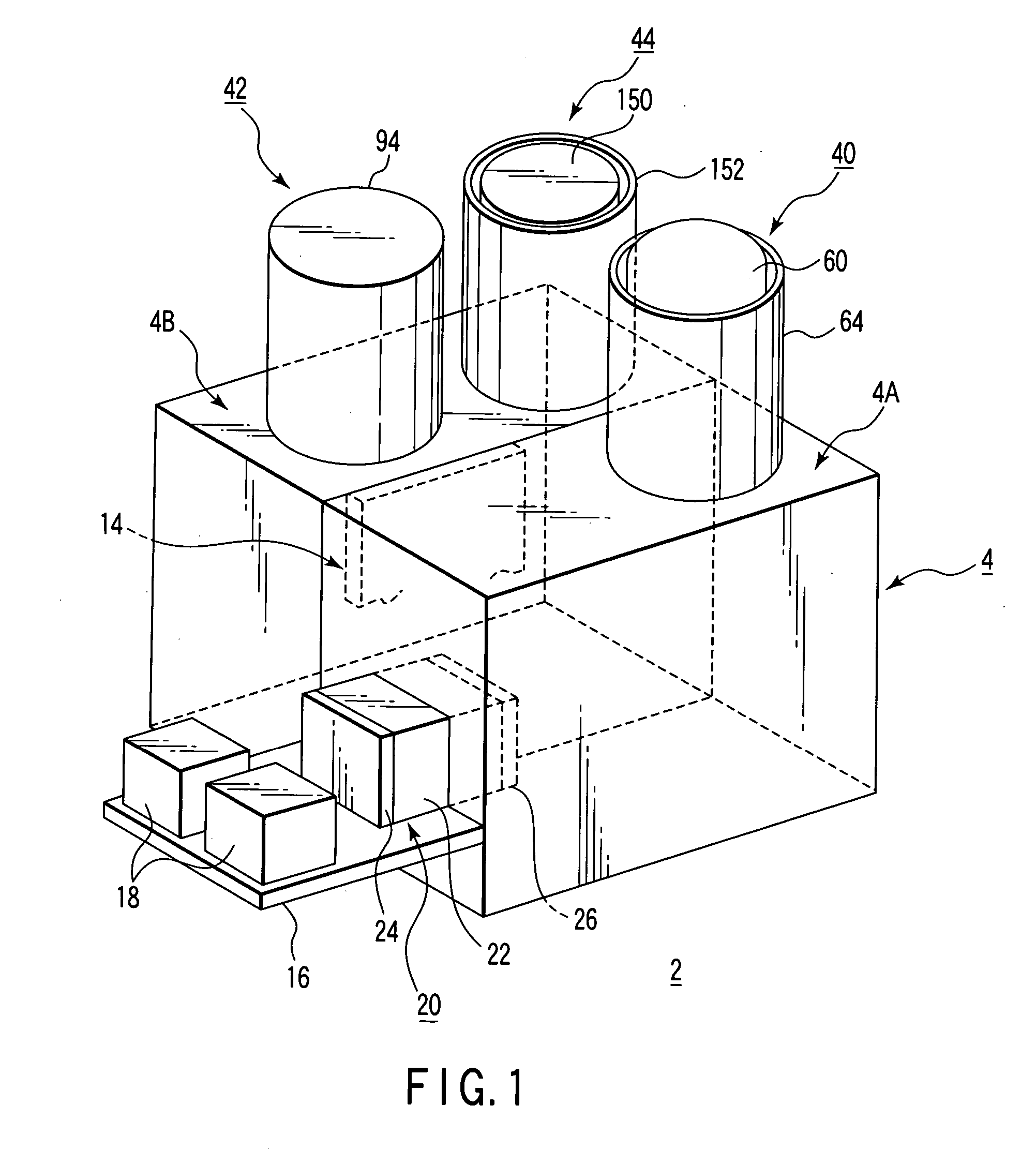
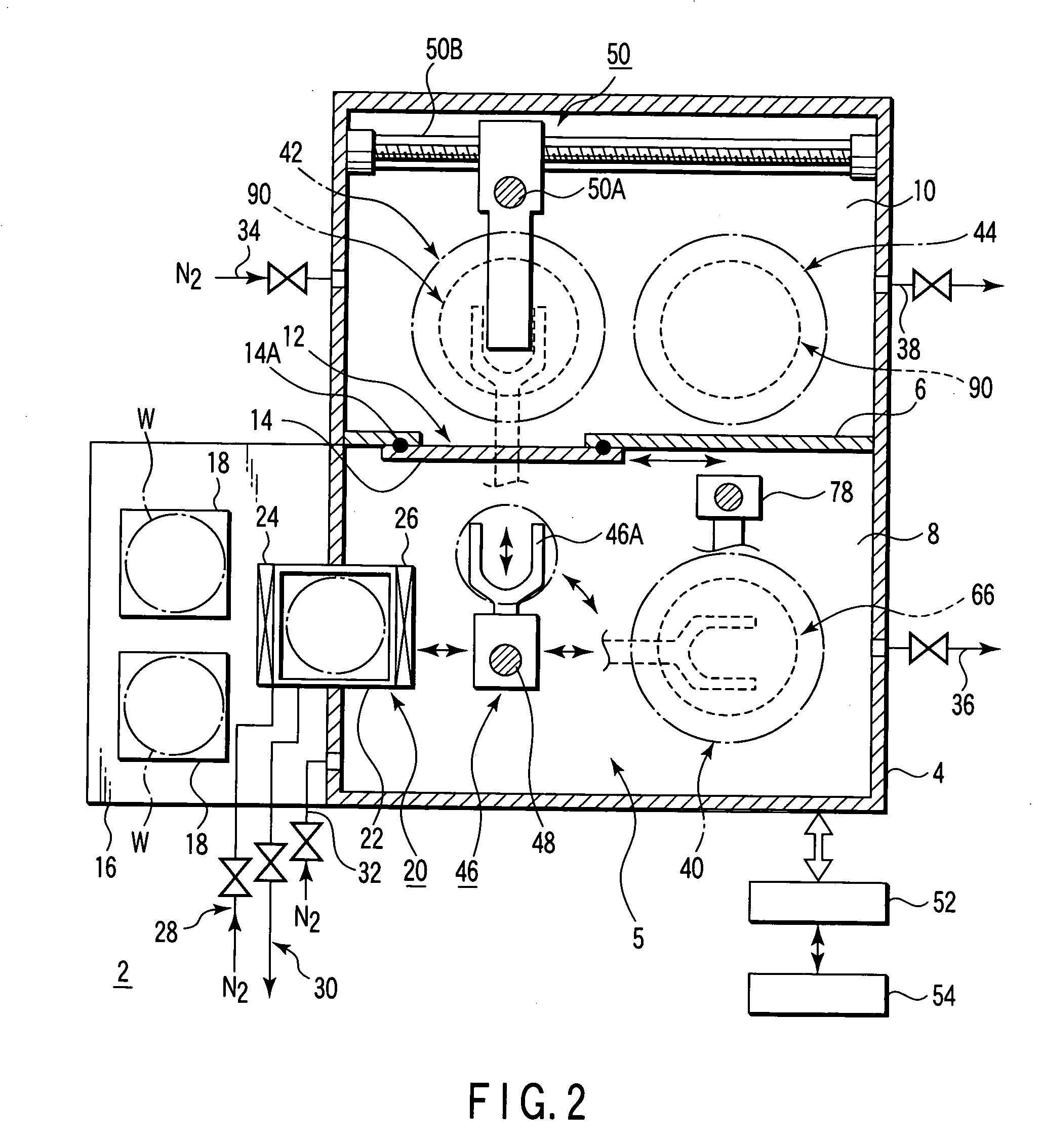
[0056]FIG. 1 is a perspective view schematically showing a semiconductor processing system according to a first embodiment of the present invention. FIG. 2 is a sectional plan view schematically showing the processing system shown in FIG. 1. As shown in FIGS. 1 and 2, this processing system 2 includes an airtight casing 4 formed of a cubic or rectangular box as a whole. The casing 4 defines therein an airtight handling area 5 for handling semiconductor wafers (typically made of silicon) as target objects. The casing 4 is made of a metal material, such as aluminum, with the inner surface covered with a corrosion resistant coating, such as an alumite coating (aluminum oxide). The casing 4 may be made of another metal, such as stainless steel.

[0057] As shown in FIG. 2, the handling area 5 is airtightly divided by a partition wall 6 into two rooms, i.e., a main-process area 8 and a pre-process area 10. The partition wall 6 is made of a metal mate...

second embodiment

[0126] [Semiconductor Processing System]

[0127]FIG. 13 is a perspective view schematically showing a semiconductor processing system according to a second embodiment of the present invention. FIG. 14 is a sectional plan view schematically showing the processing system shown in FIG. 13. The processing system 230 according to the second embodiment includes a pre-processing apparatus (vertical batch pre-processing apparatus) 232, which is a combination of a film transformation apparatus 42 according to the first embodiment with a heat-processing function.

[0128] Specifically, the processing system 230 includes an airtight casing 4X having a shape formed such that the portion corresponding to the heat-processing apparatus 44 (see FIG. 1) is removed from the casing 4 shown in FIG. 1. As shown in FIG. 14, the casing 4X defines therein an airtight handling area 5X for handling semiconductor wafers (typically made of silicon) as target objects. The handling area 5X is formed of a main-proces...

third embodiment

[0145] [Semiconductor Processing System]

[0146]FIG. 17 is a perspective view schematically showing a semiconductor processing system according to a third embodiment of the present invention. FIG. 18 is a sectional plan view schematically showing the processing system shown in FIG. 17. The processing system 260 according to the third embodiment includes a pre-processing apparatus 262, which has the same function as the pre-processing apparatus 232 according to the second embodiment, but is disposed on one side of a casing 4Y.

[0147] Specifically, the processing system 260 includes an airtight casing 4Y having a shape formed such that the portion corresponding to the pre-process area 10 is removed from the casing 4 shown in FIG. 1. As shown in FIG. 18, the casing 4Y defines therein an airtight handling area 5Y for handling semiconductor wafers (typically made of silicon) as target objects, which is formed only of the same main-process area 8 as that shown in FIG. 2. The pre-processing ...


PUM

PropertyMeasurementUnit
frequencyaaaaaaaaaa
frequencyaaaaaaaaaa
frequencyaaaaaaaaaa

Abstract

A vertical batch processing apparatus is configured to transform a semiconductor oxide film on target objects into an intermediate film, which is decomposed or sublimated more easily than the semiconductor oxide film, so as to remove the semiconductor oxide film. The apparatus includes a first process gas supply circuit having a first supply port disposed outside a process field to supply a first process gas, and a second process gas supply circuit having a second supply port disposed between the first supply port and the process field to supply a second process gas. A plasma generation field is disposed between the first and second supply ports to activate the first process gas to produce first active species. The first active species react with the second process gas and thereby produce a reactant to react with the semiconductor oxide film to form the intermediate film.

Description

CROSS-REFERENCE TO RELATED APPLICATIONS [0001] This application is based upon and claims the benefit of priority from prior Japanese Patent Application No. 2005-043245, filed Feb. 18, 2005, the entire contents of which are incorporated herein by reference. BACKGROUND OF THE INVENTION [0002] 1. Field of the Invention [0003] The present invention relates to a vertical batch processing apparatus used for removing a semiconductor oxide film present on target objects, such as semiconductor wafers, and a semiconductor processing system including the apparatus. The term “semiconductor process” used herein includes various kinds of processes which are performed to manufacture a semiconductor device or a structure having wiring layers, electrodes, and the like to be connected to a semiconductor device, on a target object, such as a semiconductor wafer or a glass substrate used for an LCD (Liquid Crystal Display) or FPD (Flat Panel Display), by forming semiconductor layers, insulating layers,...

Claims


Application Information

Patent Timeline
Patent Type & Authority Applications(United States)
IPC IPC(8): C23C16/00
CPCH01L21/31116H01L21/67757Y10S414/139Y10S414/14H01L21/22
Inventor MATSUURA, HIROYUKI
Owner TOKYO ELECTRON LTD
Why Eureka
Try Eureka