Thin film transistor array substrate, manufacturing method thereof, and mask

a technology of thin film transistors and array substrates, applied in the direction of originals for photomechanical treatment, instruments, optics, etc., can solve the problems of significant production cost of thin film transistor array substrates for liquid crystal display panels, and achieve the effect of reducing manufacturing costs and improving yield

Active Publication Date: 2006-08-24
LG DISPLAY CO LTD
View PDF4 Cites 30 Cited by
  • Summary
  • Abstract
  • Description
  • Claims
  • Application Information

AI Technical Summary

Benefits of technology

[0019] An object of the present invention is to provide a thin film transistor array substrate, and a manufacturing method thereof that implements a three-mask process, thereby reducing manufacturing cost and improving yield.

Problems solved by technology

Since fabricating a thin film transistor array substrate requires multiple masking processes, manufacturing a thin film transistor array substrate is significant in the production costs of a liquid crystal display panel.

Method used


Image

  • Thin film transistor array substrate, manufacturing method thereof, and mask
  • Thin film transistor array substrate, manufacturing method thereof, and mask
  • Thin film transistor array substrate, manufacturing method thereof, and mask

Examples


Embodiment Construction

[0050] Reference will now be made in detail to the preferred embodiments of the present invention, examples of which are illustrated in the accompanying drawings.

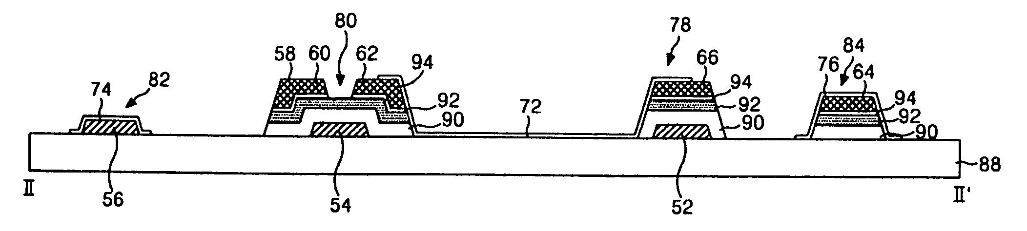
[0051]FIG. 4 is a partial plan view of an exemplary thin film transistor array substrate according to the present invention, and FIG. 5 is a cross sectional view of the exemplary thin film transistor array substrate of FIG. 4 along II-II′ according to the present invention. In FIGS. 4 and 5, a thin film transistor array substrate may include gate lines 52 and data lines 58 on a lower substrate 88, whereby a gate insulating pattern 90 may electrically insulate crossings of the gate and data lines 52 and 58. A thin film transistor 80 may be provided at each intersection of the gate and data lines 52 and 58, and a pixel electrode 72 may be provided within each liquid crystal cell defined by the crossing of the gate and data lines 52 and 58. The thin film transistor array substrate may further include storage capacitors 78 at ...


PUM

PropertyMeasurementUnit
insulatingaaaaaaaaaa
areaaaaaaaaaaa
transparentaaaaaaaaaa

Abstract

A thin film transistor array substrate including a gate pattern having a gate electrode, a gate line connected to the gate electrode, and a gate pad connected to the gate line, a source / drain pattern having a source electrode, a drain electrode, a data line connected to the source electrode, and a data pad connected to the data line, a gate insulating pattern formed along a matrix pattern including the gate pattern and the source / drain pattern except for a pixel area, a semiconductor pattern formed on the gate insulating pattern having a same pattern as the gate insulating pattern and partially removed at a thin film transistor area and the gate line area, and a transparent electrode pattern having a pixel electrode formed at the pixel area and connected to the drain electrode, a gate pad protective electrode formed on the gate pad, and a data pad protective electrode formed on the data pad.

Description

[0001] The present invention claims the benefit of Korean Patent Application No. P2002-21053 filed in Korea on Apr. 17, 2002, which is hereby incorporated by reference. BACKGROUND OF THE INVENTION [0002] 1. Field of the Invention [0003] The present invention relates to a thin film transistor array substrate, and more particularly, to a thin film transistor array substrate in a liquid crystal display device and its manufacturing method and mask used in the manufacturing method. [0004] 2. Description of the Related Art [0005] In general, liquid crystal display (LCD) devices control light transmittance using application of an electric field to produce an image. The LCD devices commonly include a liquid crystal panel having liquid crystal cells arranged in a matrix, and a driving circuit for driving the liquid crystal cells. [0006] The liquid crystal display panel includes a thin film transistor array substrate and an opposing color filter array substrate, wherein spacers are positioned...

Claims


Application Information

Patent Timeline
Patent Type & Authority Applications(United States)
IPC IPC(8): H01L21/84H01L29/04G03F1/14G02F1/1333H01L21/77H01L27/12
CPCG02F2001/136236H01L27/1288H01L27/1214G03F1/144G03F1/50G03F1/70H01L27/124H01L27/1222H01L27/1255G02F1/136236G02F1/1333
Inventor KIM, WOONG KWONCHO, HEUNG LYUL
Owner LG DISPLAY CO LTD
Why Eureka
Try Eureka