CMOS image sensor for reducing partition noise

a technology of image sensor and partition noise, which is applied in the field of cmos image sensor for reducing partition noise, can solve the problems of partition noise, multiple transfer transistors, and the inability of all channel electrons to move, so as to reduce partition noise, reduce partition noise, and shorten the falling time

Inactive Publication Date: 2006-08-24
INTELLECTUAL VENTURES II
View PDF9 Cites 19 Cited by
  • Summary
  • Abstract
  • Description
  • Claims
  • Application Information

AI Technical Summary

Benefits of technology

[0023] It is, therefore, an object of the present invention to provide a CMOS image sensor for reducing a partition noise caused by a short falling time of a transfer control signal applied to a gate of a transfer transistor.
[0024] In accordance with an aspect of the present invention, there is provided a CMOS image sensor including: a unit pixel, including a transfer transistor controlled by a transfer control signal; and a transfer control signal controller for controlling a rising and a falling times of the transfer control signal, wherein the falling time of the transfer control signal is sufficiently increased to reduce a partition noise.
[0025] In accordance with another aspect of the present invention, there is provided a CMOS image sensor including: a plurality of unit pixels arranged in a column X a row form, each including a transfer transistor controlled by a transfer control signal; and a transfer control signal controller for controlling a rising and a falling times of the transfer control signal; and a plurality of capacitive parts connected between a ground voltage and a common node which is connected between an output terminal of the transfer control signal controller and gates of the transfer transistors to thereby increase the falling time of the transfer transistor when the transfer transistors contained in the unit pixels of the same row are turned off, wherein, the plural unit pixels are disposed in the same row being controlled by the single transfer control signal controller.

Problems solved by technology

Meanwhile, the transfer transistor TX has several problems when a transfer control signal applied to a gate of a transfer transistor is dropped from a logic level ‘HIGH’ to a logic level ‘LOW’, that is, when it changes from a turned-on state to a turned-off state.
The biggest problem is a partition noise caused by a charge injection to the floating diffusion node FD, which occurs due to a short falling time of the transfer control signal.
However, since the turn-off time of the transfer transistor TX is very short, all channel electrons cannot move to the floating diffusion node ND.
Therefore, when seen from the outside, it appears that noise occurs.
Since the partition noise is considered as noise on a screen, it acts as a factor that degrades a performance of the image sensor.

Method used


Image

  • CMOS image sensor for reducing partition noise
  • CMOS image sensor for reducing partition noise
  • CMOS image sensor for reducing partition noise

Examples


embodiment 1

[0049] A first embodiment is to increase the falling time of the transfer control signal applied to the gate of the transfer transistor by reducing a W / L ratio of an NMOS transistor of the CMOS type driver DRV.

[0050]FIGS. 7A to 7C are circuit diagrams describing a driver for controlling the transfer transistor in accordance with the first embodiment of the present invention.

[0051] A CMOS inverter type driver illustrated in FIG. 7A includes a PMOS transistor P and an NMOS transistor N connected in series between a power voltage VDD and a ground voltage VSS. The CMOS inverter type driver receives an input signal IN through gates of the two transistors to output an inverted signal OUT.

[0052] It is assumed that the W / L ratio of the NMOS transistor N is K, a resistance can be increased, i.e., a current is decreased, by increasing the length L or decreasing the width W, thereby increasing the falling time of the transfer control signal.

[0053] Meanwhile, the width W of the gate electro...

embodiment 2

[0061] A second embodiment is to increase a falling time (τ) of a transfer transistor by increasing a capacitance C.

[0062]FIGS. 9 and 10 are diagrams depicting a CMOS type driver for driving a transfer transistor in accordance with a second embodiment of the present invention.

[0063] As shown, the CMOS image sensor includes a plurality of unit pixels P1 to P1280 and a CMOS type driver DRV. Each of the unit pixels P1 to P1280 includes a photodiode, a floating diffusion node, a transfer transistor, a reset transistor, a drive transistor, and a select transistor. The CMOS type driver DRV controls the on operation and the off operation of the transfer transistors TX1 to TX1280 contained in the unit pixels.

[0064] A CMOS inverter type driver is illustrated as an example of the CMOS type driver DRV. The plurality of unit pixels P1 to P1280 are disposed in a single row. Accordingly, the CMOS type driver DRV simultaneously controls the plurality of transfer transistors TX1 to TX1280 of the...

embodiment 3

[0071] The layout can be designed more simply by partially revising the structure of the first embodiment.

[0072]FIGS. 11A to 11C are circuit diagrams showing a driver for controlling a transfer transistor in accordance with a third embodiment of the present invention.

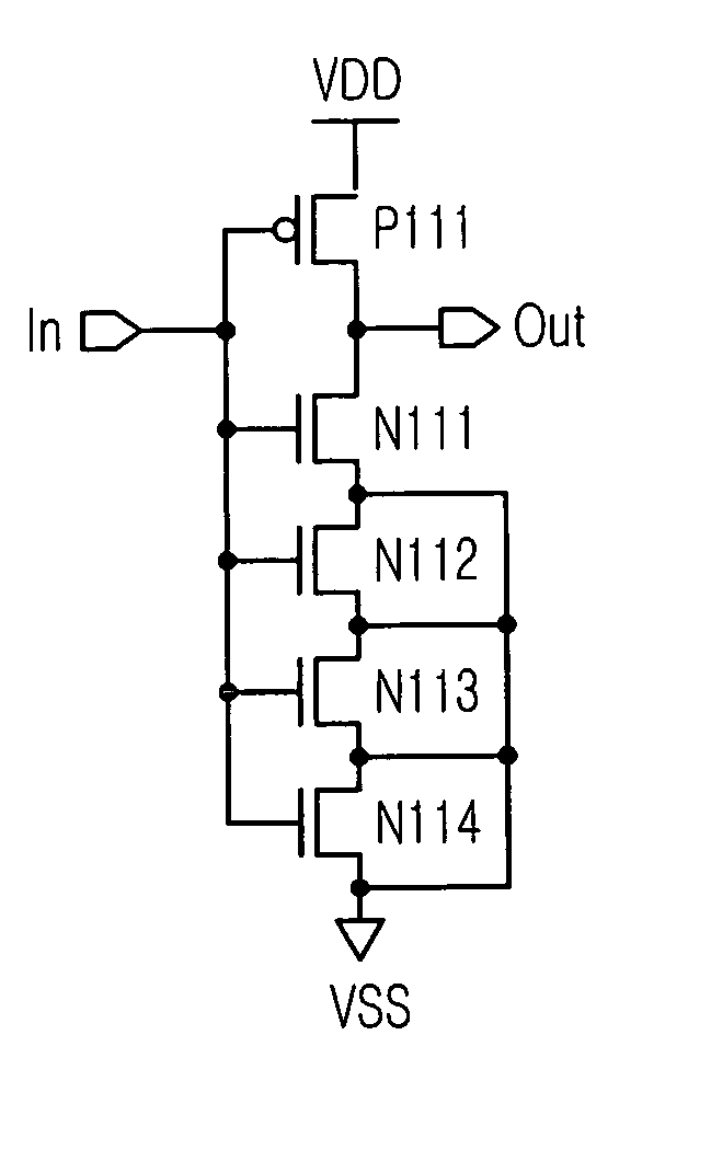
[0073] As shown, a CMOS inverter type driver includes one PMOS transistor P111 and four NMOS transistors N111 to N114 connected in series.

[0074] Although a basic structure is similar to the structure of FIG. 7C, sources of the NMOS transistors N111 to N114 are commonly connected to a ground voltage VSS, thereby forming a kind of a resistor.

[0075] In FIG. 11A, sources of the NMOS transistors N111 to N114 are commonly connected to the ground voltage VSS. In FIG. 11B, sources of the NMOS transistors N112 to N114 are commonly connected to the ground voltage VSS. In FIG. 11C, no sources of the NMOS transistors are connected to the ground voltage VSS.

[0076] In FIGS. 11A to 11C, the NMOS transistors are formed as many as ...


PUM


Abstract

A CMOS image sensor according to an embodiment of the present invention includes a unit pixel, including a transfer transistor controlled by a transfer control signal; and a transfer control signal controller for controlling a rising and a falling times of the transfer control signal, wherein the falling time of the transfer control signal is sufficiently increased to reduce a partition noise.

Description

FIELD OF THE INVENTION [0001] The present invention relates to a CMOS image sensor; and, more particularly, to a CMOS image sensor for reducing a partition noise by extending a falling time of a transfer control signal applied to a gate of a transfer transistor. DESCRIPTION OF THE RELATED ART [0002] An image sensor is a semiconductor device that converts an optical image into an electric signal. The image sensor is classified into a charge coupled device (hereinafter, referring to a CCD) image sensor and a complementary metal oxide semiconductor (hereinafter, referring to a CMOS) image sensor. [0003] The CCD image sensor includes at least one. The MOS capacitors are arranged very close to one another, and charge carriers are stored in the MMOS capacitors and transferred thereto. [0004] On the contrary, the CMOS image sensor includes a plurality of unit pixels fabricated through CMOS processes. Each of the unit pixels includes one photodiode and three or four MOS transistors for driv...

Claims


Application Information

Patent Timeline
Patent Type & Authority Applications(United States)
IPC IPC(8): H01L31/06H01L27/146H04N5/335H04N5/357H04N5/369H04N5/374
CPCH01L27/14601H04N5/3651H04N25/671H01L27/146
Inventor BAE, CHANG-MINSHIM, KYUNG-JIN
Owner INTELLECTUAL VENTURES II
Why Eureka
Try Eureka