Check patentability & draft patents in minutes with Patsnap Eureka AI!

Differential to single-ended converter

a converter and single-ended technology, applied in the field of electronic converters, can solve the problems of reducing the common mode rejection ratio of the converter, asymmetry, and burdening the approach, and achieve the effect of large common mode rejection ratio (cmrr)

Inactive Publication Date: 2006-08-24
STMICROELECTRONICS SRL
View PDF6 Cites 2 Cited by
  • Summary
  • Abstract
  • Description
  • Claims
  • Application Information

AI Technical Summary

Benefits of technology

The invention is a differential to single-ended converter that has excellent performance in RF applications. It has a high common mode rejection ratio and matches the load impedance in a wide frequency range. Compared to existing converters, it provides better trade-offs between bandwidth, CMRR, and silicon area requirement. The converter allows for the conversion of a differential signal into a single-ended signal with a substantially unitary gain without a decrease in voltage level. It uses a differential pair of identical transistors and a circuit for filtering DC components. Unlike other converters, it does not require a transformer and includes a current generator and degeneration resistors to achieve equal gains for each input node. The differential pair is configured as a source follower.

Problems solved by technology

This approach is burdened by the following drawbacks that limit its use:
the impedance matching network MN includes resonant circuits and it is not possible to ensure a precisely determined output impedance over a relatively wide range of frequencies;
the parasitic capacitances of the integrated transformer are not negligible and cause an asymmetry that reduces the common mode rejection ratio of the converter (CMRR).
A drawback of this converter is that only the signal on a single collector of the differential pair is used, thus the voltage level of the output single-ended signal is halved.
Furthermore, the output signal may be corrupted by noise on the supply lines or generated by the bias current generator.

Method used


Image

  • Differential to single-ended converter
  • Differential to single-ended converter
  • Differential to single-ended converter

Examples


Embodiment Construction

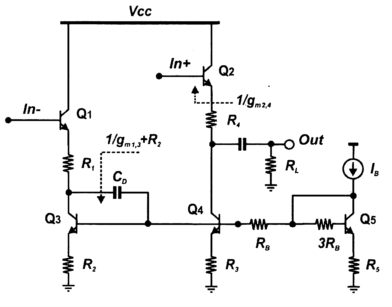
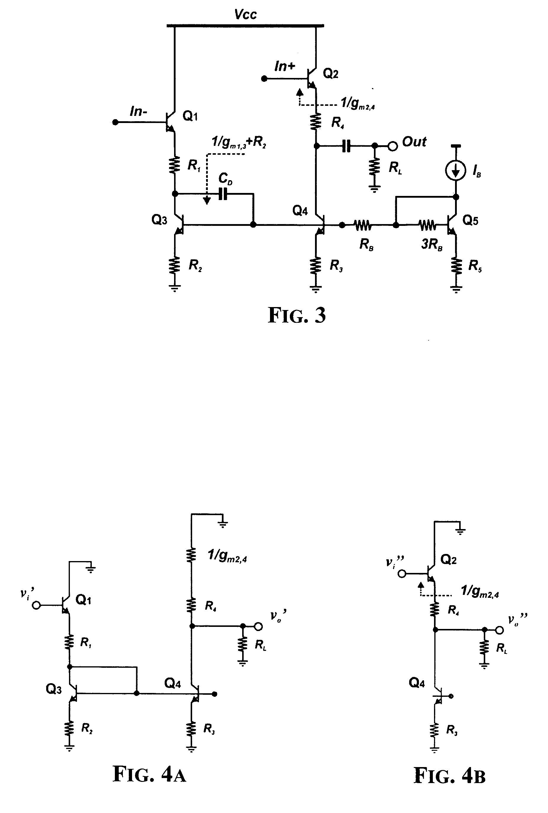
[0022] An embodiment of the converter of this invention is depicted in FIG. 3. By way of example, the converter is realized in BJT technology, but the considerations that will be made apply mutatis mutandis to a similar converter realized in MOS technology and to equivalent circuits in which the conductivity type of the transistors employed is reversed. The converter employs a differential pair of transistors Q1, Q2 in an emitter follower configuration, each biased by a respective current generator Q3, Q4. Preferably, these current generators are implemented by mirroring the two transistors Q3, Q4 to a same transistor Q5 biased with a reference current IB.

[0023] Resistors R2, R3 and R5 are dimensioned such that the gain of the converter for each of the two input nodes be the same. Resistor R4 is used for matching the output impedance and its value is determined by the following equation: RL=R4+1gm⁢ ⁢2,4(2)

The two resistors R2 and R3 must satisfy the following equation:

R2·gm2,4=R...


PUM


Abstract

A converter is for a differential input signal into a single-ended output signal and may include a differential pair of identical first and second transistors driven by the differential input signal, and a circuit for filtering DC components, connected between the current terminal of the second transistor not in common with the first transistor of the differential pair and an output node of the converter on which the single-ended output signal is generated. The converter generates a single-ended signal without employing a transformer, in lieu thereof the converter may include a current generator biasing the differential pair by of third and fourth output transistors, in a current mirror configuration, connected in series with the first and second transistors, respectively. The converter may also include degeneration resistors of the transistors of the current mirror, dimensioned such that the gains of the converter for each of the two input nodes of the differential signal are equal and of opposite sign.

Description

FIELD OF THE INVENTION [0001] This invention relates to electronic converters, and, more particularly, to a differential to single-ended converter. BACKGROUND OF THE INVENTION [0002] Internal signals of integrated circuits are processed in a differential mode for enhancing rejection of noise coming from the supply lines and from the silicon substrate. It is often necessary to provide these circuits with an output stage that converts the differential signal to a single-ended signal to reduce the number of pins and to simplify the printed circuit board (PCB). [0003] Moreover, especially in RF applications, this output stage should match the load impedance for maximizing the power delivered to the load. FIG. 1 depicts a typical architecture of a differential to single-ended converter for RF applications. The circuit includes a differential pair of transistors input with the differential signal to be converted, and a transformer that provides a single-ended version of the input differen...

Claims


Application Information

Patent Timeline
Patent Type & Authority Applications(United States)
IPC IPC(8): H03F3/45H03G3/12
CPCH03F3/45174H03F3/45085H03F3/3088
Inventor COPANI, TINOSMERZI, SANTO ALESSANDROGIRLANDO, GIOVANNIPALMISANO, GIUSEPPE
Owner STMICROELECTRONICS SRL
Features
  • R&D
  • Intellectual Property
  • Life Sciences
  • Materials
  • Tech Scout
  • Unparalleled Data Quality
  • Higher Quality Content
  • 60% Fewer Hallucinations
Learn More