LDMOS device and method of fabrication of LDMOS device

a metal oxide semiconductor and lateral double diffusion technology, applied in the field of semiconductor devices, can solve the problems of bd /sub>tend to adversely affect the ron and vice versa, the device will typically exhibit low power loss in high voltage applications, and the ron tends to increase, so as to achieve the effect of reducing the ron and reducing the breakdown voltag

Active Publication Date: 2006-08-24
MACRONIX INT CO LTD
View PDF5 Cites 12 Cited by
  • Summary
  • Abstract
  • Description
  • Claims
  • Application Information

AI Technical Summary

Benefits of technology

[0011] In accordance with the present invention, a well region having an SSR well profile is produced within an LDMOS device, such that a doping concentration within the well region changes with depth so as to provide a lighter doping concentration in a surface region of the well region than in a region below the surface region of the well region. This results in an SSR well region which provides a lighter surface doping to enable a higher breakdown voltage to be obtained within the LDMOS device, and heavier sub-surface doping to decrease the Ron.
[0012] In the past, super steep retrograde profiles have been produced in the channel region of a MOS device to alleviate what is referred to as the “reverse short channel effect” (an adverse effect on threshold voltage resulting from decreasing the channel length beyond a certain point). This is discussed for example in U.S. Pat. No. 6,444,550 B1 and in the article “Front-End Trends, Challenges, and Potential Solutions for the 180-100 nm IC Technology Generations” by Peter M Zeitzoff, Sematech Inc, Austin Tex., USA, Semiconductor Fabtech—10th Edition, pages 275-280.
[0013] In one embodiment, the step (b) comprises the step of implanting at least one element in the substrate to form the well region, with the depth of implantation being controlled so as to produce the SSR well profile. The depth of implantation can be controlled, for example, by controlling the implantation energy. This enables the doping profile within the SSR well region, and in particular the depth at which doping concentration transitions from a lighter to a heavier doping concentration, to be managed so as to meet the requirements of a particular implementation.

Problems solved by technology

By designing LDMOS devices with low on-resistance and high breakdown voltage, such devices will typically exhibit low power loss in high voltage applications.
One problem when designing such LDMOS devices is that techniques and structures that tend to maximise Vbd tend to adversely affect the Ron and vice versa.
However, this lighter concentration well doping tends to increase the Ron.

Method used


Image

  • LDMOS device and method of fabrication of LDMOS device
  • LDMOS device and method of fabrication of LDMOS device
  • LDMOS device and method of fabrication of LDMOS device

Examples


Embodiment Construction

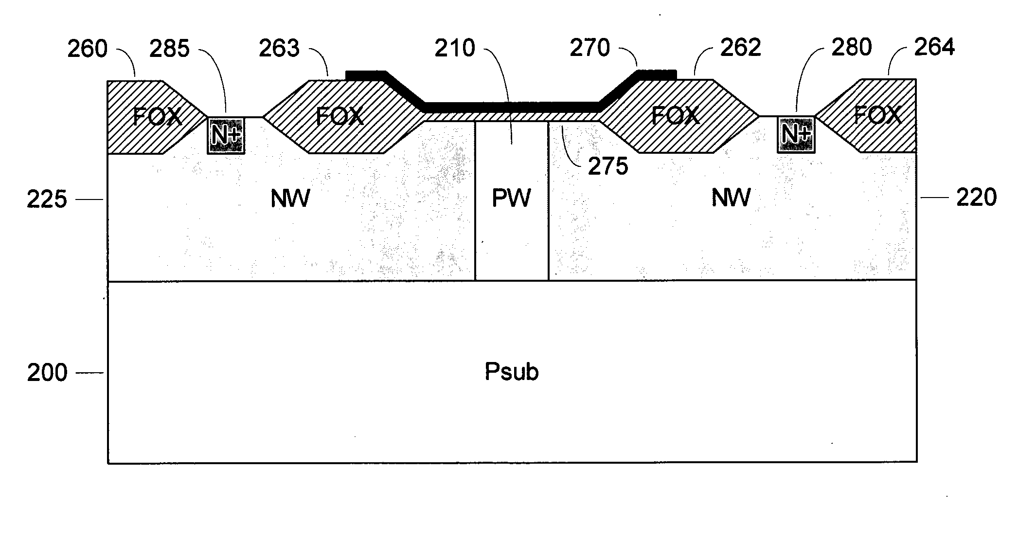
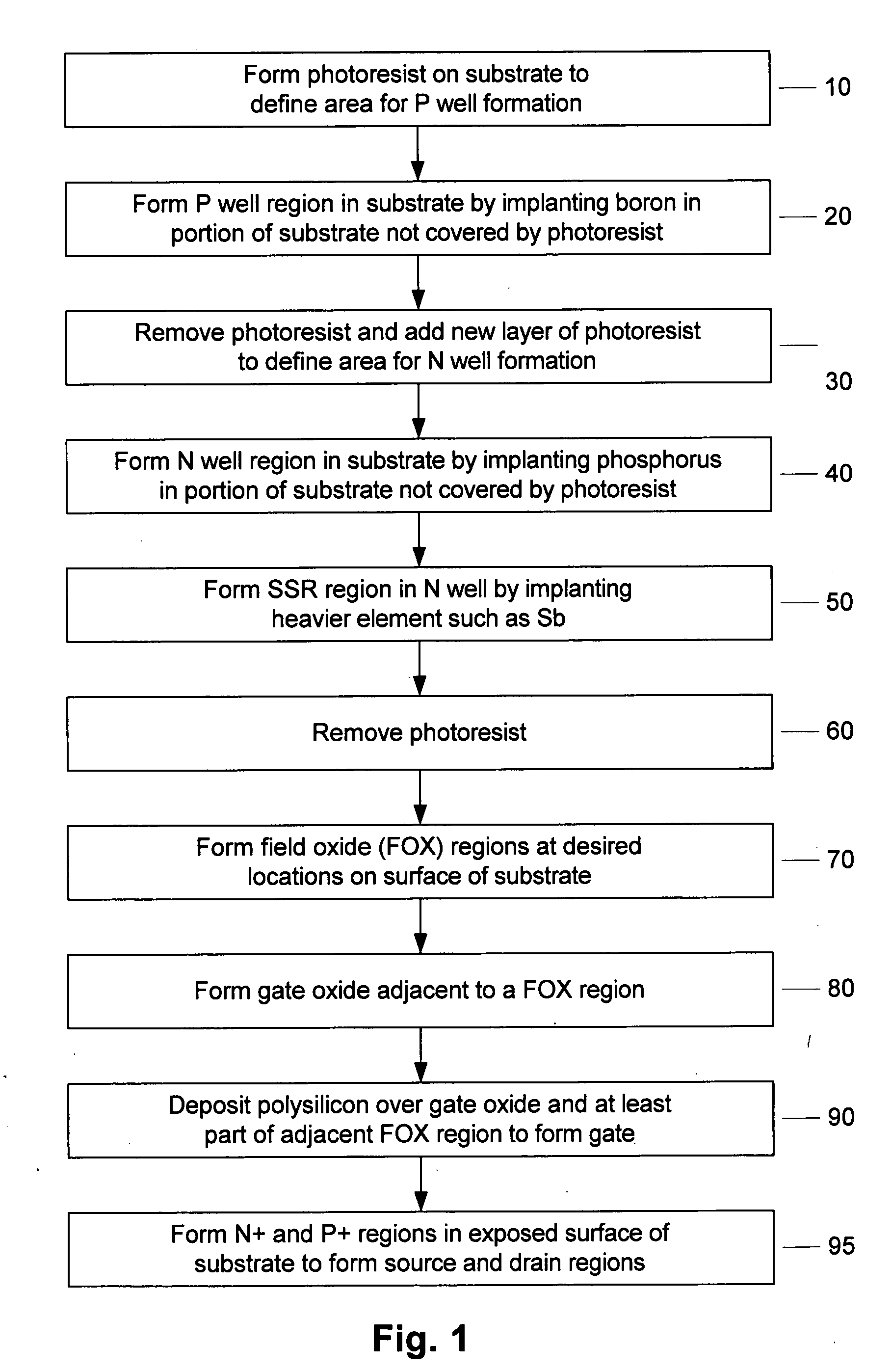
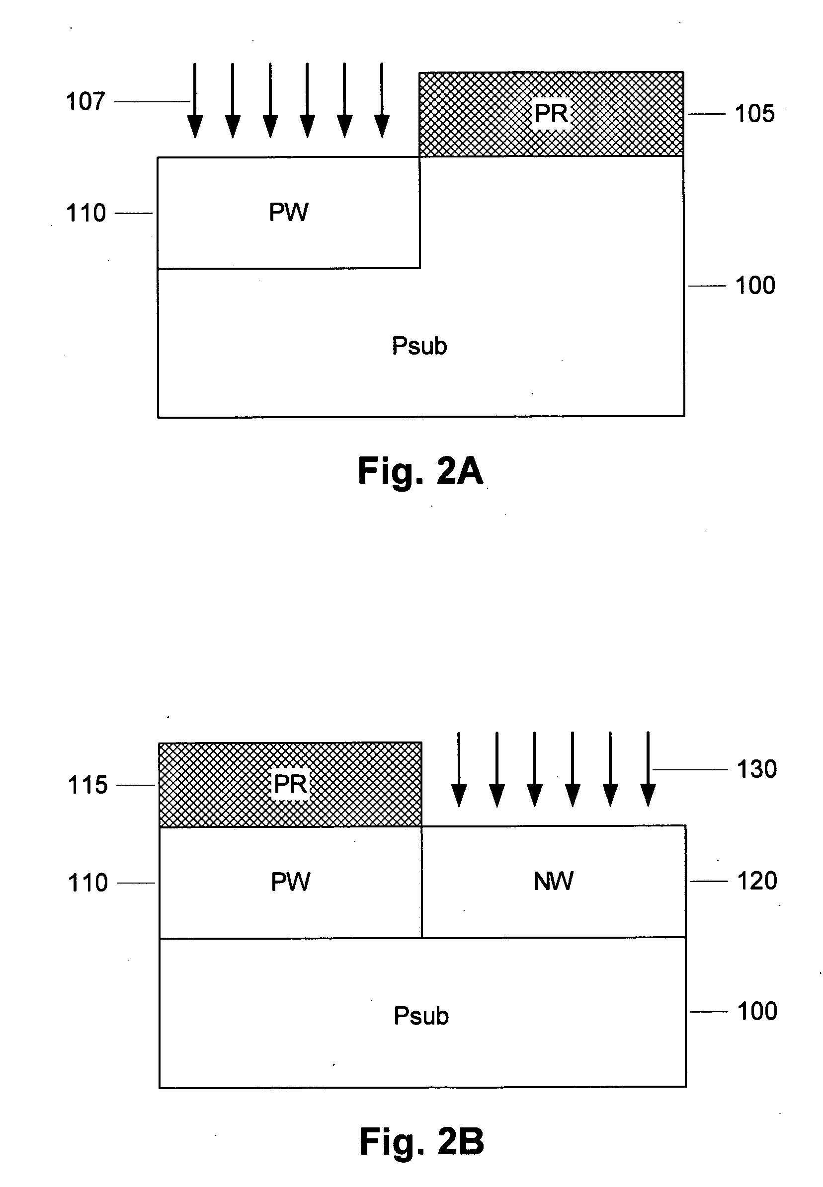
[0030] According to one embodiment of the invention, an LDMOS device having a low on-resistance whilst exhibiting a high breakdown voltage is provided. A method of fabricating such an LDMOS device in accordance with one embodiment of the present invention will now be discussed with reference to FIG. 1. For the purposes of describing the embodiment of FIG. 1, it is assumed that the substrate is a P-type substrate, and the SSR well profile is to be formed in an N-type well region. However, it will be appreciated by those skilled in that art that the dopant types of the various regions can be changed so as to produce P-type devices instead of N-type devices, and vice versa. Hence, in an alternative embodiment, the substrate may be an N-type substrate and the SSR well profile may be formed within a P-type well region.

[0031] Considering now FIG. 1, at step 10 a photoresist is formed on the P-type substrate to define an area in which a P-type well region (P well) is to be formed. In part...


PUM


Abstract

A lateral double diffused metal oxide semiconductor (LDMOS) device, and method of fabricating such a device, are provided. The method comprises the steps of: (a) providing a substrate of a first conductivity type; (b) forming within the substrate a well region of a second conductivity type, the well region having a super steep retrograde (SSR) well profile in which a doping concentration changes with depth so as to provide a lighter doping concentration in a surface region of the well region than in a region below the surface region of the well region; (c) forming a gate layer which partly overlies the well region and is insulated from the well region; and (d) forming one of a source region and a drain region in the well region. The presence of the SSR well region provides a lighter surface doping to enable a higher breakdown voltage to be obtained within the LDMOS device, and heavier sub-surface doping to decrease the on-resistance.

Description

BACKGROUND OF THE INVENTION [0001] 1. Field of the Invention [0002] The present invention relates generally to semiconductor devices, and more particularly to a lateral double diffused metal oxide semiconductor (LDMOS) device and a method of fabricating such a device. [0003] 2. Description of the Prior Art [0004] LDMOS devices are typically used in high voltage applications, and when designing such LDMOS devices, it is important that the device should have a very high breakdown voltage (Vbd), whilst also exhibiting, when operating, a low on-resistance (Ron). By designing LDMOS devices with low on-resistance and high breakdown voltage, such devices will typically exhibit low power loss in high voltage applications. In addition, by exhibiting a low on-resistance, a high drain current (Idsat) can be achieved when the transistor is in saturation, which increases speed of operation of the device. One problem when designing such LDMOS devices is that techniques and structures that tend to...

Claims


Application Information

Patent Timeline
Patent Type & Authority Applications(United States)
IPC IPC(8): H01L21/336H01L29/76
CPCH01L29/0847H01L29/167H01L29/42368H01L29/66659H01L29/7835H01L29/0878H01L29/78627
Inventor HSU, CHIA-LUNLIU, MU-YILU, TAO-CHENGYANG, ICHENCHEN, KUAN-PO
Owner MACRONIX INT CO LTD
Why Eureka
Try Eureka