Substrate removal process for high light extraction LEDs

a technology of high light extraction and substrate removal, which is applied in the direction of semiconductor devices, basic electric elements, electrical appliances, etc., can solve the problems of reducing the overall emission efficiency of the device, and difficulty in emitted light from the led to the surroundings

Active Publication Date: 2006-08-24
CREELED INC
View PDF70 Cites 310 Cited by
  • Summary
  • Abstract
  • Description
  • Claims
  • Application Information

AI Technical Summary

Benefits of technology

[0009] The present invention provides a method for fabricating a solid state light emitting device, such as an LED, wherein the substrate is removed, which provides a number of advantages as fully described below. One embodiment of a method for fabricating semiconductor based light emitting devices according to the present invention comprises providing a plurality of semiconductor light emitting devices on a substrate wafer, each of said emitting dev

Problems solved by technology

LEDs are efficient at generating light, but the light has difficulties emitting from the LED to the surroundings because of the differences in the indexes of refraction between the LED material and surroundings.
The remainder of the light is trapped within the structure of the LED, and can eventually become absorbed into the semiconductor material, which reduces the overall emitting efficiency of the LED.
Light can become trapped within t

Method used


Image

  • Substrate removal process for high light extraction LEDs
  • Substrate removal process for high light extraction LEDs
  • Substrate removal process for high light extraction LEDs

Examples


Embodiment Construction

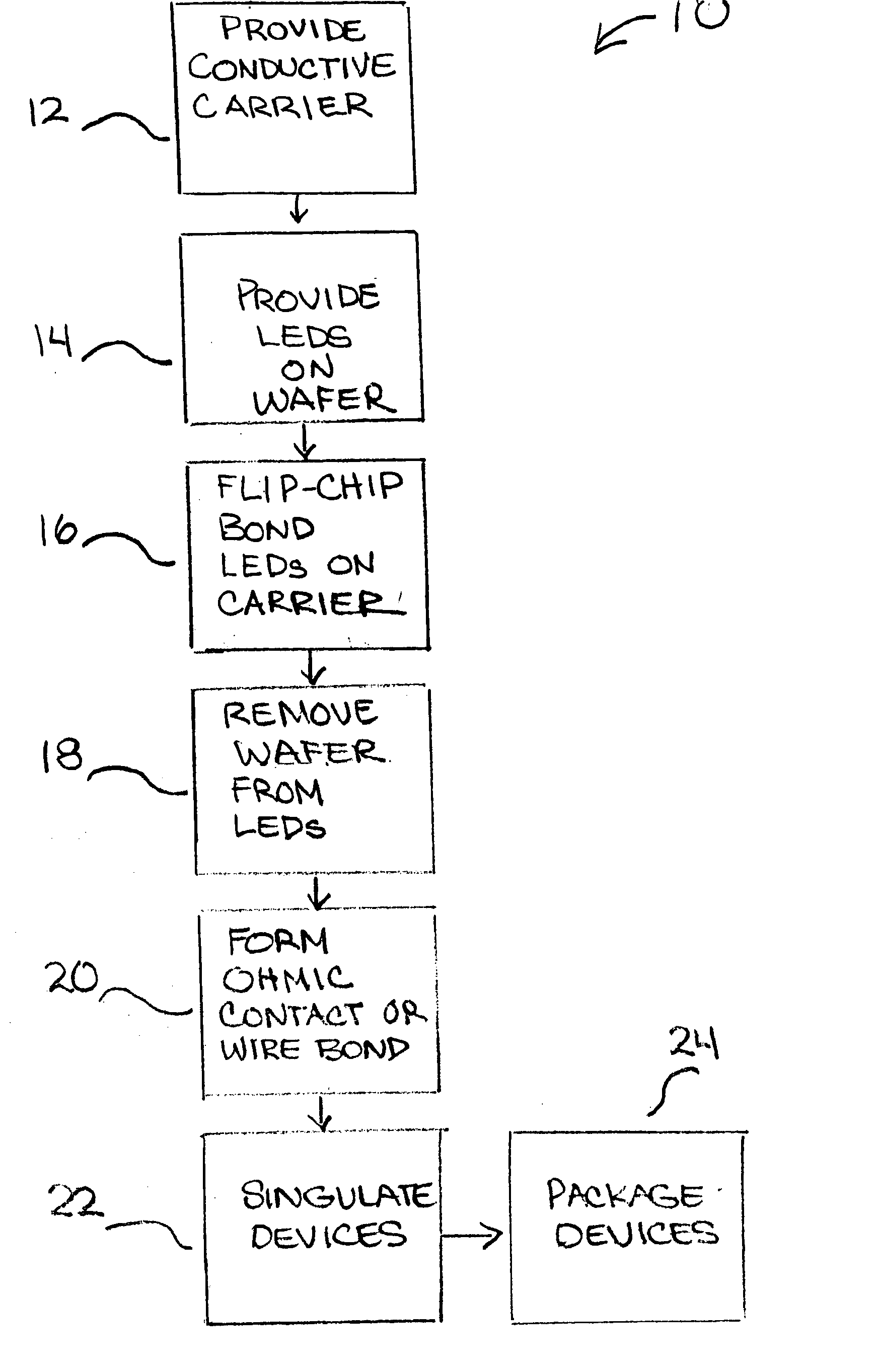
[0025]FIG. 1 shows one embodiment of a method 10 according to the present invention for fabricating light emitting semiconductor devices, with the method 10 particularly adapted to fabricating singulated vertical geometry light emitting diodes (LEDs) on a submount / carrier (“carrier”) with the substrate on each LED removed. In one embodiment of the method 10, LEDs are made from the Group-III nitride material system, such as AlGaN / GaN, and are fabricated on a conductive carrier. In step 12, a conductive carrier is provided that is sized such that a plurality of LEDs can be mounted on one of its lateral surfaces. Desirable characteristics of the carrier are low cost, low resistivity, good thermal conductivity, and good coefficient of thermal expansion relative to the bonded devices.

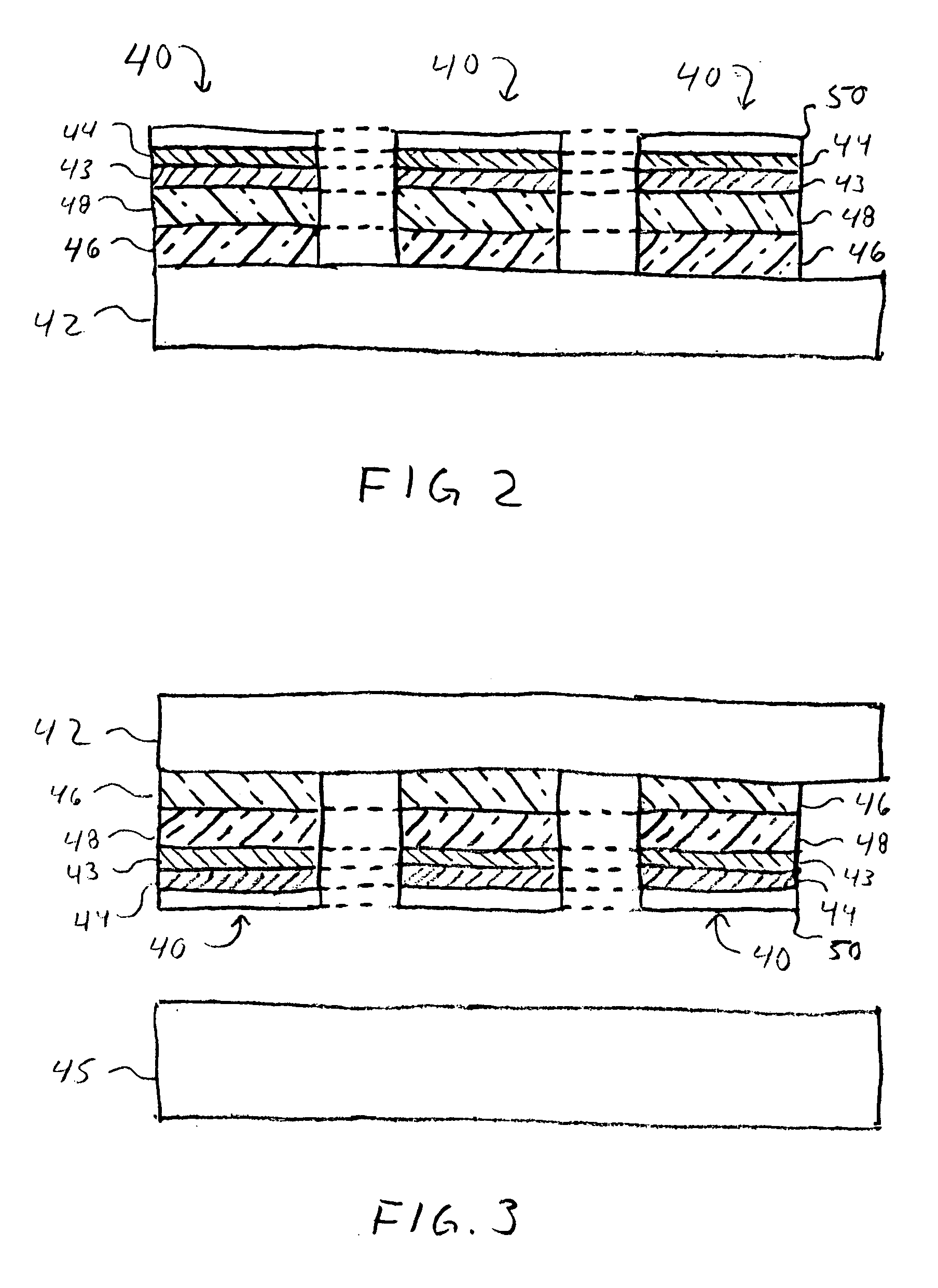
[0026] Many different types of carriers can be used having different structures. In one embodiment, the carrier can comprise a semiconductor material, such as SiC or Si, and to provide low resistivity chara...


PUM


Abstract

A method for fabricating light emitting diode (LEDs) comprises providing a plurality of LEDs on a substrate wafer, each of which has an n-type and p-type layer of Group-III nitride material formed on a SiC substrate with the n-type layer sandwiched between the substrate and p-type layer. A conductive carrier is provided having a lateral surface to hold the LEDs. The LEDs are flip-chip mounted on the lateral surface of the conductive carrier. The SiC substrate is removed from the LEDs such that the n-type layer is the top-most layer. A respective contact is deposited on the n-type layer of each of the LEDs and the carrier is separated into portions such that each of the LEDs is separated from the others, with each of the LEDs mounted to a respective portion of said carrier.

Description

BACKGROUND OF THE INVENTION [0001] 1. Field of the Invention [0002] This invention relates to a method for fabricating a semiconductor device, and more particularly to a method for fabricating a light emitting semiconductor device on a conducting carrier. [0003] 2. Description of the Related Art [0004] Improvements in the manufacturing of semiconductor materials in the Group-III nitride material system has helped advance the development of GaN / AlGaN opto-electronic devices such as high efficiency blue, green and ultra-violet (UV) light emitting diodes (LED or LEDs) and lasers, and electronic devices such as high power microwave transistors. Some of the advantages of GaN is its 3.4 eV wide direct bandgap, high electron velocity (2×107 cm / s), high breakdown field (2×10⁶ V / cm) and the availability of heterostructures. [0005] Typical LEDs can comprise a p-type doped layer and an n-type doped layer such that when a bias is applied across the doped layers the LED emits light. Other LEDs c...

Claims


Application Information

Patent Timeline
IPC IPC(8): H01L21/78H01L21/301H01L21/46H01L33/00
CPCH01L33/0079H01L33/007H01L33/0093
Inventor EDMOND, JOHN
Owner CREELED INC
Why Eureka
Try Eureka