Differential signal connector with wafer-style construction

a technology of wafer-style construction and differential signal connector, which is applied in the direction of high frequency circuit adaptation, coupling device connection, cross-talk/noise/interference reduction, etc., can solve the problems of reducing the design, manufacture and installation of reliable connectors, reducing and reducing the size of electronic devices and systems. , to achieve the effect of enhancing the high speed transmission ability of connectors and high speed operation of connectors

Active Publication Date: 2006-08-24
MOLEX INC
View PDF31 Cites 77 Cited by
  • Summary
  • Abstract
  • Description
  • Claims
  • Application Information

AI Technical Summary

Benefits of technology

[0008] Yet another object of the present invention is to provide a stacked receptacle connector that enables differential signal pairs to be installed into a connector body using individual inserts in the form of wafers, each of which is relatively easy to manufacture and each of which also allows ground planes to be provided between each wafer insert in an encompassing connector housing.
[0011] A still further object of the present invention is to provide a unique circuit board layout for accommodating the tail portions of connectors of the structure described above, which circuit board layout facilities the high speed operation of connectors of the invention.
[0012] Yet another object of the present invention is to provide a circuit board with a particular arrangement of traces that enhance the high speed transmission abilities of the connectors of the invention, the circuit board having a plurality of conductive traces extending to mounting through holes disposed in a circuit board, the through holes being arranged in a pattern such that a plurality of ground traces encompass a pair of differential signal traces, and in which the ground traces are arranged at the corners of a four-sided figure, with the differential signal through holes arranged in line within a perimeter defined by the ground through holes.
[0016] The halves of the signal terminal wafer inserts have serrated-style bases on which are formed alternating projections and recesses, with the projections of the first of the two insert wafer halves being received within the recesses of the second of the two signal insert wafer halves and vice-versa. In this manner the terminal tails portions are easily arranged in a line in the edge-to-edge fashion stated above.

Problems solved by technology

Over the last several years, however, electronic devices and systems have gotten both smaller and faster, making reliable connectors more difficult to design, manufacture and install onto printed circuit boards.

Method used


Image

  • Differential signal connector with wafer-style construction
  • Differential signal connector with wafer-style construction
  • Differential signal connector with wafer-style construction

Examples


Embodiment Construction

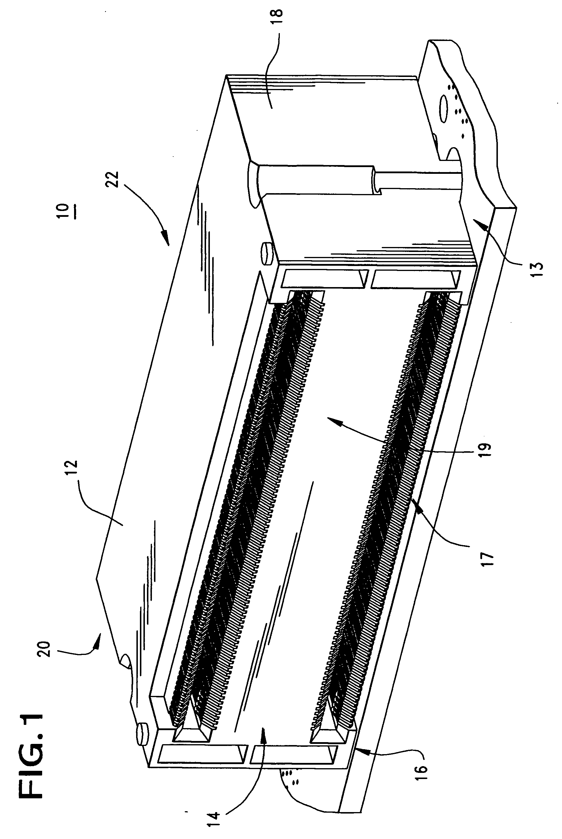
[0043] Referring now to FIG. 1, there is shown a perspective view of a connector 10 that is constructed in accordance with the principles of the present invention. The connector 10 has a top surface 12, a front face 14, a bottom surface 16 and left and right side surfaces, or faces, 18 and 20. As can be seen in FIG. 1, the connector 10 front face has two receptacle portions 17 and 19 disposed thereon into which a circuit board, device or blade connector may be inserted and by which electrical signals can be carried to or extended from a circuit board 13 to which the base connector 10 is attached. The connector 10 of the present invention is a compressible attachment-style connector, meaning that it is attached to a circuit board by means of through hole pins, that as explained below, are shown in the embodiment depicted as compliant pins.

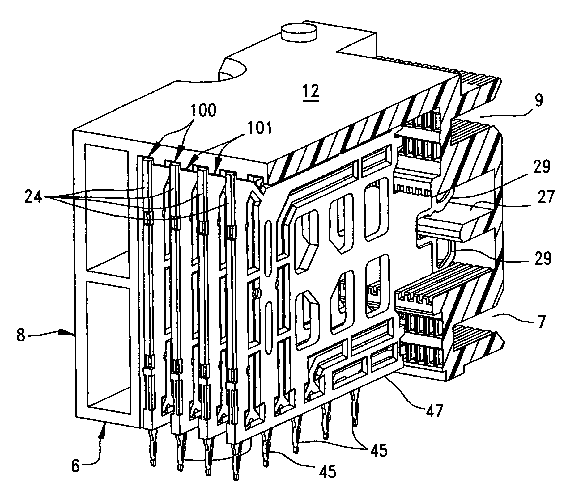
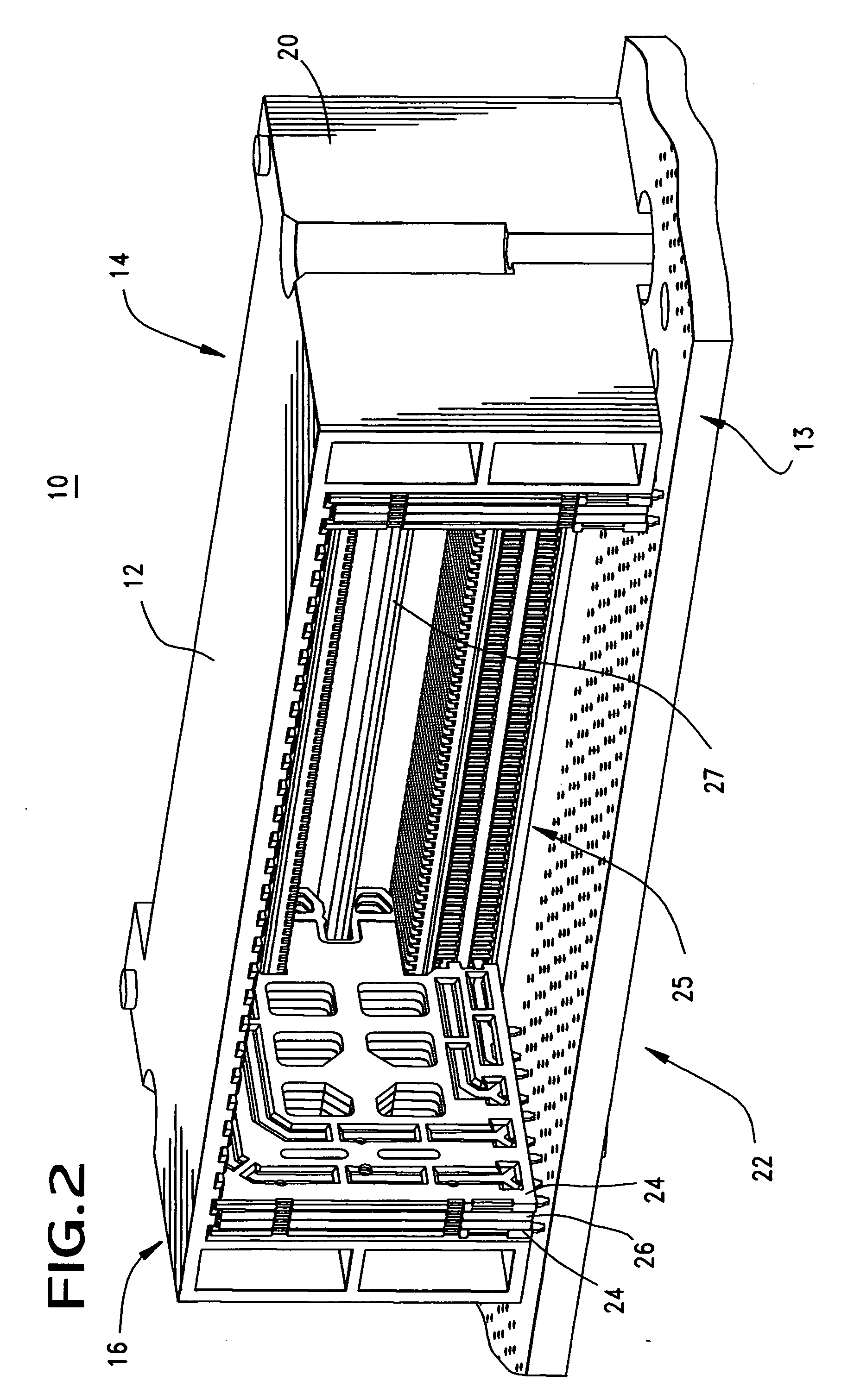
[0044] The connector also has a rear face 20, which is shown more clearly in FIG. 2, which is a perspective view of the connector 10 of FIG. 1, bu...


PUM


Abstract

Stacked receptacles in a connector that each provide side-by-side differential signal contacts, are attached to a circuit board without additional width to accommodate multiple layers of differential signals by using connector wafer inserts that rotate the side-by-side positioned differential signal contacts to front-to-back contacts.

Description

REFERENCE TO RELATED APPLICATIONS [0001] This application claims priority from U.S. Provisional Patent Application No. 60 / 655,051, filed Feb. 22, 2005. BACKGROUND OF THE INVENTION [0002] This invention relates generally to high speed connectors that are used as vertically stacked receptacle connectors, and more particularly, to connectors utilizing insert wafers that incorporate differential signal terminals which are positioned alongside each other where they appear in the connector receptacle portions and which are turned at their tail portions for joining to a printed circuit board. [0003] Electrical connectors are well known to those of ordinary skill in the electronic arts as generally reliable devices by which electrical signal paths can be extended into and obtained from a printed circuit board. Over the last several years, however, electronic devices and systems have gotten both smaller and faster, making reliable connectors more difficult to design, manufacture and install ...

Claims


Application Information

Patent Timeline
Patent Type & Authority Applications(United States)
IPC IPC(8): H01R13/648
CPCH01R12/724H01R13/6464H01R13/6587H05K1/0219H05K1/0237H05K1/0245H05K1/116H05K3/429H05K2201/09236H05K2201/09618H05K2201/09718H05K2201/09809H05K2201/10189
Inventor AVERY, HAZELTON P.CASHER, PATRICK R.NELSON, RICHARD A.REGNIER, KENT E.
Owner MOLEX INC
Why Eureka
Try Eureka