Nitride semiconductor light emitting device

a light-emitting device and semiconductor technology, applied in solid-state devices, white arms/cold weapons, weapons, etc., can solve the problems of increasing manufacturing costs and complicating the manufacturing process of light-emitting devices, and achieve effective diffused effects, enhanced light-emitting efficiency, and reduced operating voltage

Inactive Publication Date: 2006-08-31
SAMSUNG ELECTRO MECHANICS CO LTD
View PDF5 Cites 36 Cited by
  • Summary
  • Abstract
  • Description
  • Claims
  • Application Information

AI Technical Summary

Benefits of technology

[0012] The main characteristic of the invention is that the electron diffusion layer having a multilayer structure is formed between the n-side contact layer and the active layer. The electron diffusion layer is formed by alternately stacking the first InAlGaN layer having the higher electron concentration than that of the n-side contact layer and the second InAlGaN layer ha...

Problems solved by technology

However, these approaches complicate the manufacturing process of the light emitting device and increa...

Method used


Image

  • Nitride semiconductor light emitting device
  • Nitride semiconductor light emitting device
  • Nitride semiconductor light emitting device

Examples


Embodiment Construction

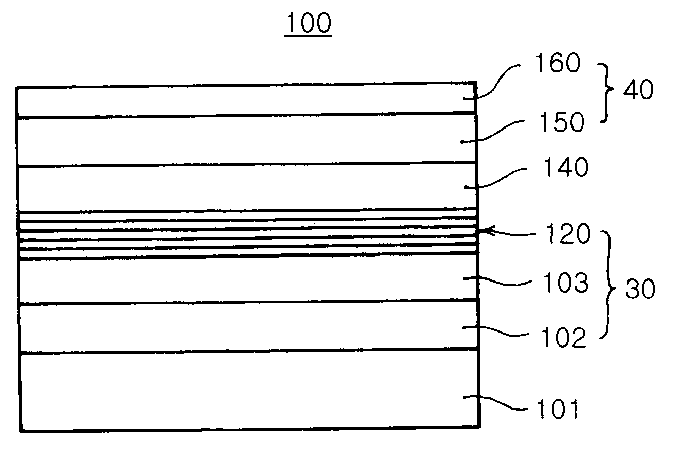
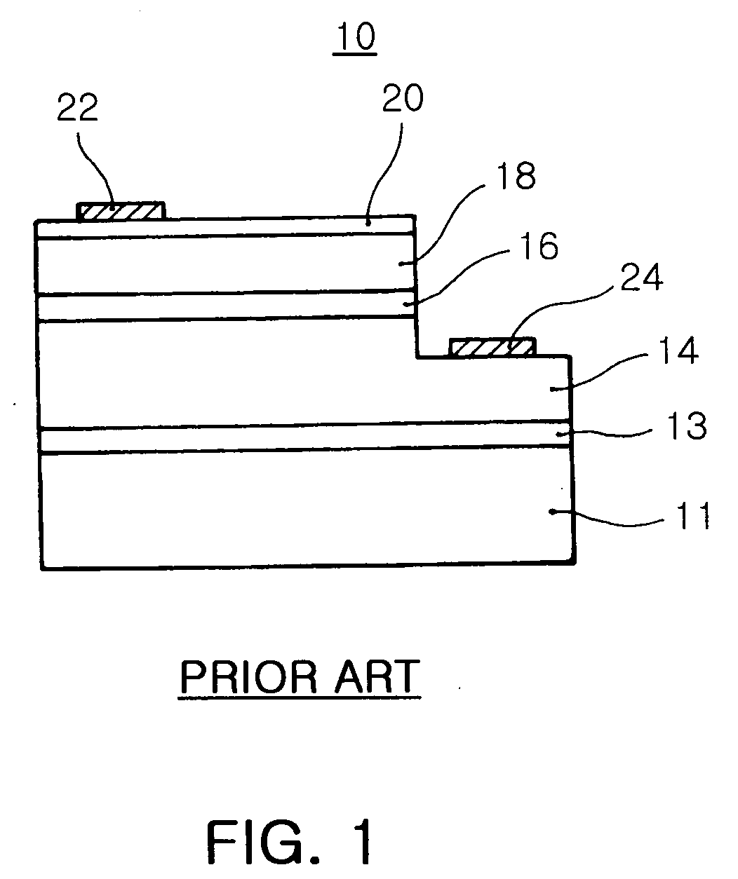
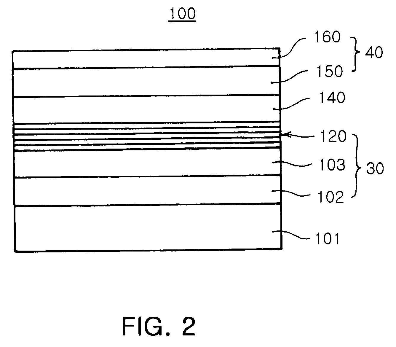
[0032] Preferred embodiments will now be described in detail with reference to the accompanying drawings. It should be noted that the embodiments of the invention can take various forms, and that the present invention is not limited to the embodiments described herein. The embodiments of the invention are described so as to enable those having an ordinary knowledge in the art to have a perfect understanding of the invention. Accordingly, shape and size of components of the invention are enlarged in the drawings for clear description of the invention. Like components are indicated by the same reference numerals throughout the drawings.

[0033]FIG. 2 is a cross-sectional view illustrating a nitride semiconductor light emitting device according to one embodiment of the invention. Referring to FIG. 2, the nitride semiconductor light emitting device 100 comprises an undoped GaN layer 102, an n-side contact layer 103, a current diffusion layer 120, an active layer 140, and a p-type clad la...


PUM


Abstract

Provided is a nitride semiconductor light emitting device having enhanced output power and resistance to electrostatic discharge. The light emitting device comprises an n-side contact layer formed on a substrate, a current diffusion layer formed on the n-side contact layer, an active layer formed on the current diffusion layer, and a p-type clad layer formed on the active layer. The current diffusion layer is formed by alternately stacking at least one first InAlGaN layer having a higher electron concentration than that of the n-side contact layer and at least one second InAlGaN layer having a lower electron concentration than that of the n-side contact layer.

Description

RELATED APPLICATION [0001] The present invention is based on, and claims priority from, Korean Application Number 2005-16524, filed Feb. 28, 2005, the disclosure of which is incorporated by reference herein in its entirety. BACKGROUND OF THE INVENTION [0002] 1. Field of the Invention [0003] The present invention generally relates to a nitride semiconductor light emitting device, and, more particularly, to a nitride semiconductor light emitting device, designed to have a low operating voltage and an enhanced tolerance to electrostatic discharge (ESD) while providing enhanced light emitting efficiency. [0004] 2. Description of the Related Art [0005] Recently, a III-V group nitride semiconductor, such as a gallium nitride (GaN) semiconductor, has been in the spotlight as an essential material for light emitting devices, such as light emitting diodes (LEDs), laser diodes (LDs), and the like, due to its excellent physical and chemical properties. In particular, LEDs or LDs manufactured u...

Claims


Application Information

Patent Timeline
IPC IPC(8): H01L33/00H01L33/04H01L33/14H01L33/32H01L33/36
CPCH01L33/04H01L33/14H01L33/32F41B11/57F41B11/68F41B11/89
Inventor WOOK SHIM, HYUNHAK WON, JONGSUB PARK, JINSEO KANG, JOONGJIN LEE, HYUN
Owner SAMSUNG ELECTRO MECHANICS CO LTD
Why Eureka
Try Eureka