

Inspection method semiconductor device and display device
a semiconductor and display device technology, applied in measurement devices, electrical testing, instruments, etc., can solve problems such as miniaturization and pixel numbers, quality problems for liquid crystal displays, and inability to normally work gate lines and data lines
- Summary
- Abstract
- Description
- Claims
- Application Information
AI Technical Summary
Benefits of technology
Problems solved by technology
Method used
Image

Examples
first embodiment
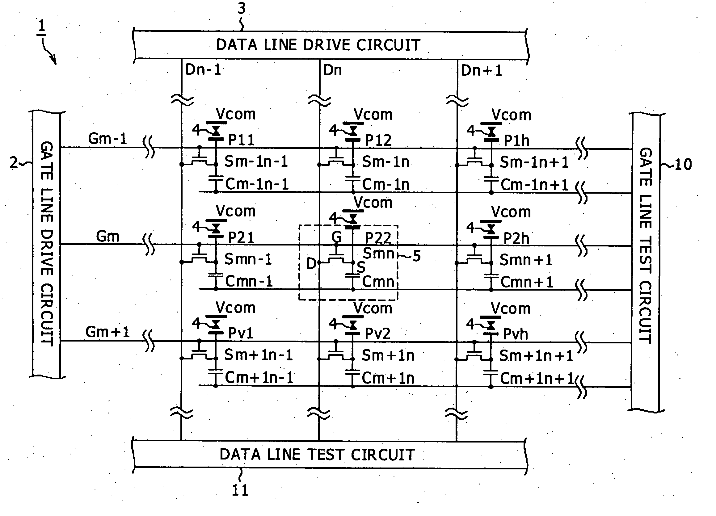
[0072] The first embodiment includes logic circuits in the data line test circuit 11 and the gate line test circuit 10 in order to test the presence of line defects. The kind of the logical operation executed by the logic circuit and which lines of the data lines or gate lines should be coupled to the logic circuit, should be determined depending on the actual interconnect layout structure on the semiconductor substrate, in consideration of obtaining adequate determination results of the test for line defects.
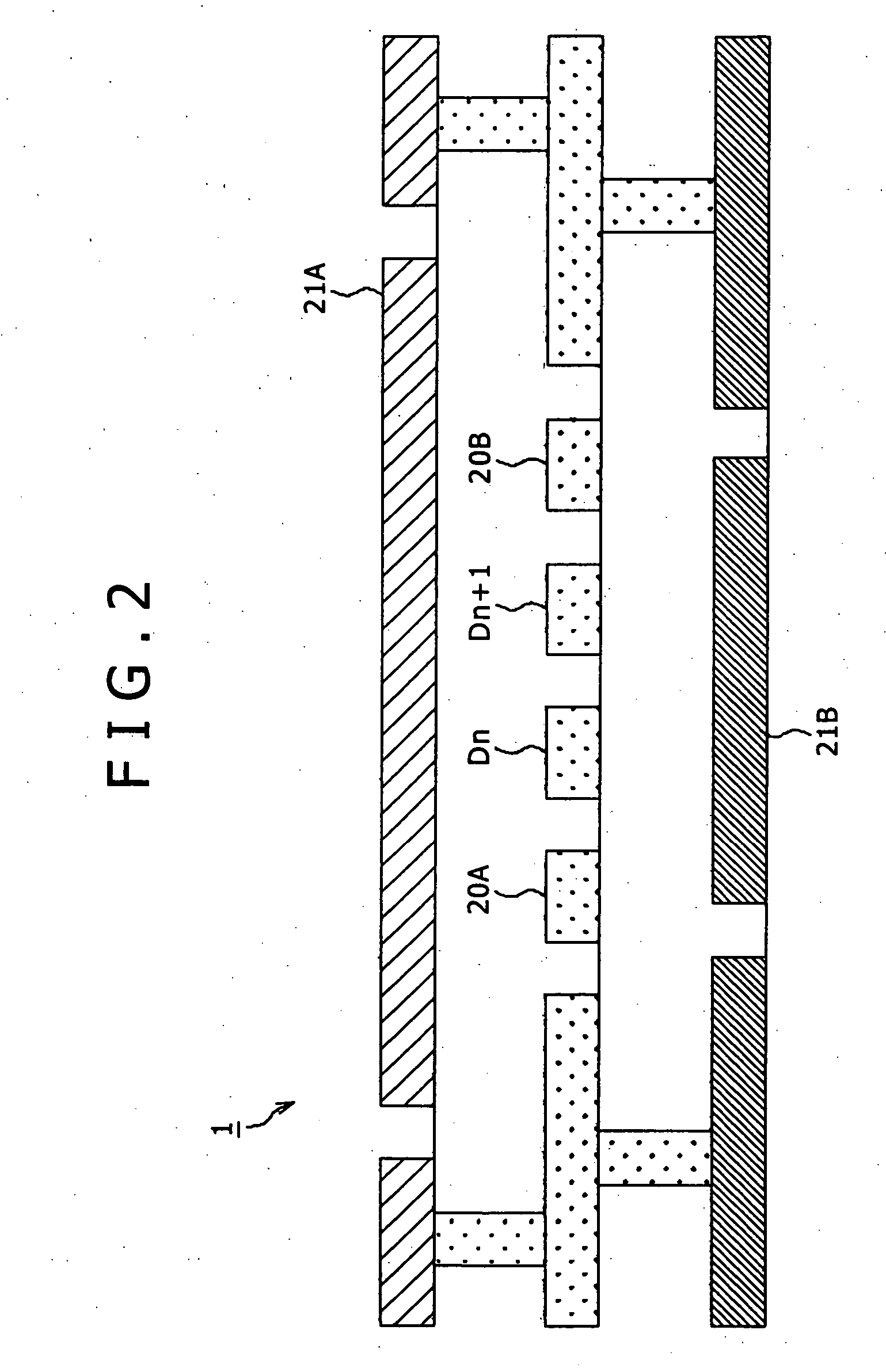
[0073]FIG. 2 illustrates an example of the interconnect layout structure on the semiconductor substrate as the liquid crystal display 1 shown in FIG. 1. This drawing illustrates as a sectional view the layout structure on the semiconductor substrate. For simplified description, FIG. 2 shows only the interconnect layout structure of the data lines, and that of the gate lines are omitted. The following specific description of the configurations for tests is based on the premise t...
second embodiment
[0181]FIG. 11 illustrates a circuit configuration example of a liquid crystal display as a first example of the present invention.
[0182] The basic configuration of the liquid crystal display 1 shown in the drawing is the same as that of each example of the first embodiment shown in FIG. 1. However, for testing the presence of line defects in data lines, the data line test circuit 11 has a different configuration as follows.
[0183] Referring to FIG. 11, the data line test circuit 11 includes a comparator 15.
[0184] The non-inverting input of the comparator 15 is coupled to an end of the data line Dn. Input to the inverting input is a reference level VREF. The output from the comparator 15 is amplified by a buffer amplifier 16, followed by being output from the test output terminal 17. Note that the outputs of the logic circuits shown in FIGS. 3, 5 and 7 in the first embodiment may be coupled to a buffer amplifier.
[0185] In this manner, the second embodiment includes a comparator cir...
PUM
 Abstract
Description
Claims
Application Information