Gate structure and a transistor having asymmetric spacer elements and methods of forming the same

a technology of gate structure and transistor, which is applied in the direction of basic electric elements, electrical equipment, semiconductor devices, etc., can solve the problems of affecting the overall performance of an integrated circuit, affecting the start of the on-state, and the maximum practical operating frequency, so as to enhance current drive capabilities, enhance transistor performance, and reduce static and dynamic leakage currents. parasitic drain capacitance, the effect of enhancing current drive capabilities

Active Publication Date: 2006-08-31
ADVANCED MICRO DEVICES INC
View PDF2 Cites 46 Cited by
  • Summary
  • Abstract
  • Description
  • Claims
  • Application Information

AI Technical Summary

Benefits of technology

[0022] Generally, the present invention is directed to a technique that enables enhancement of transistor performance by performing the halo implantation and the extension implantation in an asymmetric manner with respect to a drain and source region so as to provide enhanced current drive capabilities while reducing static and dynamic leakage currents as well as parasitic drain capacitances. Asymmetric spacer structures are employed to enhance the formation of a conductive channel, thereby improving the drive current capability of the transistor and reducing the drain / gate overlap and thus the parasitic drain / gate capacitance.

Problems solved by technology

For instance, static and dynamic leakage currents may significantly affect the overall performance of an integrated circuit, as the achievable amount of heat dissipation that is required for transistor architectures producing high dynamic and / or static leakage currents may restrict the maximum practical operating frequency.
Moreover, during the building up of the conductive channel, the parasitic capacitances caused by the overlaps 104o, 103o may require high currents for recharging the parasitic capacitor and may delay the start of the on-state, thereby degrading the raise and fall times during the switching operation.

Method used


Image

  • Gate structure and a transistor having asymmetric spacer elements and methods of forming the same
  • Gate structure and a transistor having asymmetric spacer elements and methods of forming the same
  • Gate structure and a transistor having asymmetric spacer elements and methods of forming the same

Examples


Embodiment Construction

[0032] Illustrative embodiments of the invention are described below. In the interest of clarity, not all features of an actual implementation are described in this specification. It will of course be appreciated that in the development of any such actual embodiment, numerous implementation-specific decisions must be made to achieve the developers' specific goals, such as compliance with system-related and business-related constraints, which will vary from one implementation to another. Moreover, it will be appreciated that such a development effort might be complex and time-consuming, but would nevertheless be a routine undertaking for those of ordinary skill in the art having the benefit of this disclosure.

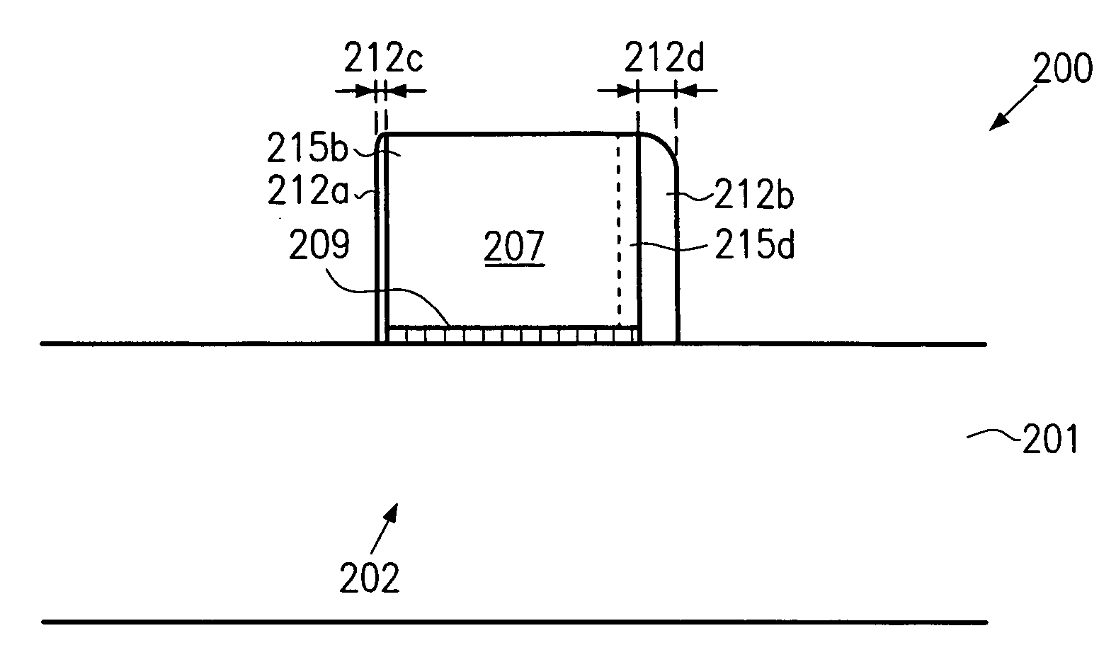
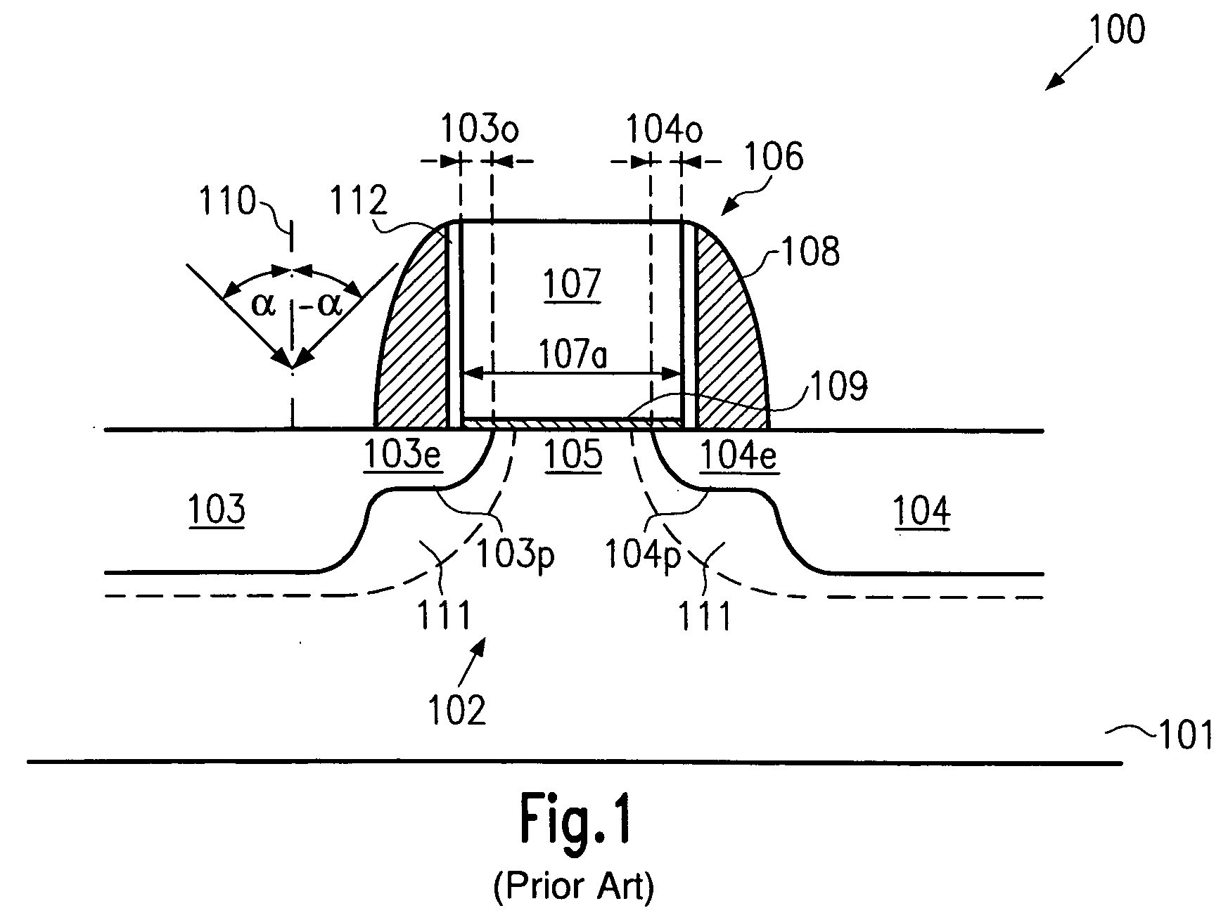
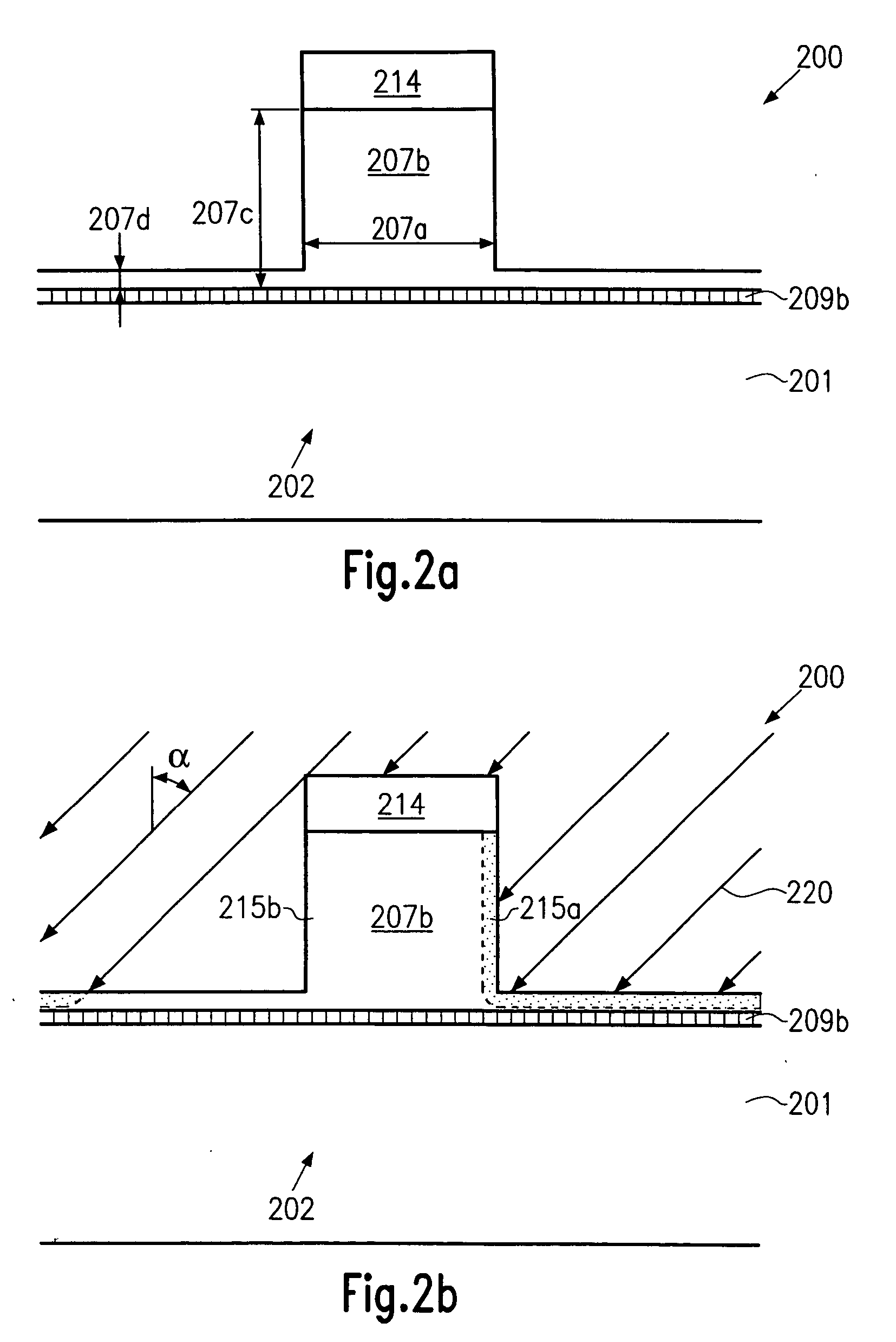
[0033] The present invention will now be described with reference to the attached figures. Various structures, systems and devices are schematically depicted in the drawings for purposes of explanation only and so as to not obscure the present invention with details that are we...


PUM


Abstract

Methods for forming asymmetric gate structures comprising spacer elements disposed on the opposed sides of a gate electrode and having a different width are disclosed. The asymmetric gate structures are employed to form an asymmetric design of a halo region and extension regions of a field effect transistor using a symmetric implantation scheme, or to further enhance the effectiveness of asymmetric implantation schemes. The transistor performance may be significantly enhanced for a given basic transistor architecture. In particular, a large overlap area may be created at the source side with a steep concentration gradient of the PN junction due to the provision of the halo region, whereas the drain overlap may be significantly reduced or may even be completely avoided to further enhance the transistor performance.

Description

BACKGROUND OF THE INVENTION [0001] 1. Field of the Invention [0002] The present invention generally relates to the fabrication of integrated circuits, and, more particularly, to the design of individual field effect transistor elements so as to enhance the performance thereof. [0003] 2. Description of the Related Art [0004] Integrated circuits typically include a large number of individual circuit elements, such as transistors, capacitors, resistors and the like. These individual circuit elements are electrically connected according to the desired circuit layout by respective conductive lines, which are mainly formed in separate “wiring” layers that are typically referred to as metallization layers. For enhancing the performance of the integrated circuit, usually the number of individual circuit elements is increased, thereby obtaining a more complex functionality of the circuit, and associated therewith the feature sizes of the individual circuit elements are reduced. [0005] Genera...

Claims


Application Information

Patent Timeline
Patent Type & Authority Applications(United States)
IPC IPC(8): H01L21/8234H01L21/336
CPCH01L21/26586H01L21/823864H01L29/66659H01L29/66772H01L29/7835H01L29/6656
Inventor WEI, ANDYBURBACH, GERTGREENLAW, DAVID
Owner ADVANCED MICRO DEVICES INC
Why Eureka
Try Eureka