Method for correcting the optical proximity effect

a technology of optical proximity and optical proximity, applied in the field of optical proximity effect correction, can solve the problems of proximity errors, undesirable and unavoidable light contributions of respective adjacent structure elements in the photosensitive layer, and often occur imaging errors, and achieve the effect of improving the quality of correction and high matching

Inactive Publication Date: 2006-08-31
QIMONDA
View PDF9 Cites 23 Cited by
  • Summary
  • Abstract
  • Description
  • Claims
  • Application Information

AI Technical Summary

Benefits of technology

[0016] Therefore, the embodiments of the invention provide an OPC correction method for use in patterning a wafer, which improves the quality of the correction. In particular, for layouts with structure elements having differing size, form and mutual distances, preferred embodiments of the invention obtain simultaneously a high match between desired and actually obtained results for the projection on the wafer.
[0028] The advantage of the use of the invention arises from the fact that mutually independent fitting procedures can be carried out from the outset for the respective structure classes or partial patterns. The problems of a uniform process model can be reduced in this case, by virtue of the fact that the accuracy of the correction is improved when using different OPC process models. An OPC model with a smaller residual error can be formed for a subset of the design structures.
[0029] The weight of the effects, which arise as a result of influences that have not been taken into account hitherto, such as resist or other process effects, thereby diminishes even if they continue to exist to a small extent. The disadvantageous influence even of long-range optical effects, such as so-called flares, which can scarcely be taken into account in the OPC process model of the prior art, can thereby be at least reduced.
[0030] The result is an improvement in the accuracy of the OPC correction and a corresponding increase in the quality of the imaging of the layout onto the wafer. This improvement in turn leads to an increase in the overall yield. The improved OPC correction may be used to produce a stored pattern that may be transferred onto a semiconductor wafer. Subsequent semiconductor processing steps are then applied to produce integrated circuits using the accurate pattern. The wafer may then be subjected to conventional back end processes such as device test, singulation and packaging to produce completed integrated circuit devices.

Problems solved by technology

In the case of high integration densities or very small structure widths, for example in the region of the resolution limit of a projection system, imaging errors often occur when transferring structures from a mask onto a wafer.
If the structure elements are particularly close together, then this may also result, in particular, in undesirable and unavoidable light contributions of respectively adjacent structure elements in the photosensitive layer.
These proximity effects, also called proximity errors, may be caused by instances of light scattering or diffractions at chromium or other absorber edges on the mask, lens imperfections, varying resist thicknesses or micro-loading effects, etc.
The imaging errors thus lead to deviations between the sizes and geometrical forms of structure elements in the pattern to be imaged which are actually formed on the wafer and those which are inherently desired by the designer in accordance with the layout that he has predefined.
However, in the present art, it is not always possible to describe the process of optically imaging the layout on the mask onto the wafer with sufficient accuracy by means of the OPC process model.
The line end shortening that occurs precisely in the case of line widths in the region of the resolution limit of the projection system often cannot be simulated simultaneously with these line widths with sufficient accuracy in the context of an OPC process model, particularly when many different line widths are present.
A correction based on this inaccurate model therefore equally supplies erroneous results.

Method used


Image

  • Method for correcting the optical proximity effect
  • Method for correcting the optical proximity effect
  • Method for correcting the optical proximity effect

Examples


Embodiment Construction

[0050] The making and using of the presently preferred embodiments are discussed in detail below. It should be appreciated, however, that the present invention provides many applicable inventive concepts that can be embodied in a wide variety of specific contexts. The specific embodiments discussed are merely illustrative of specific ways to make and use the invention, and do not limit the scope of the invention.

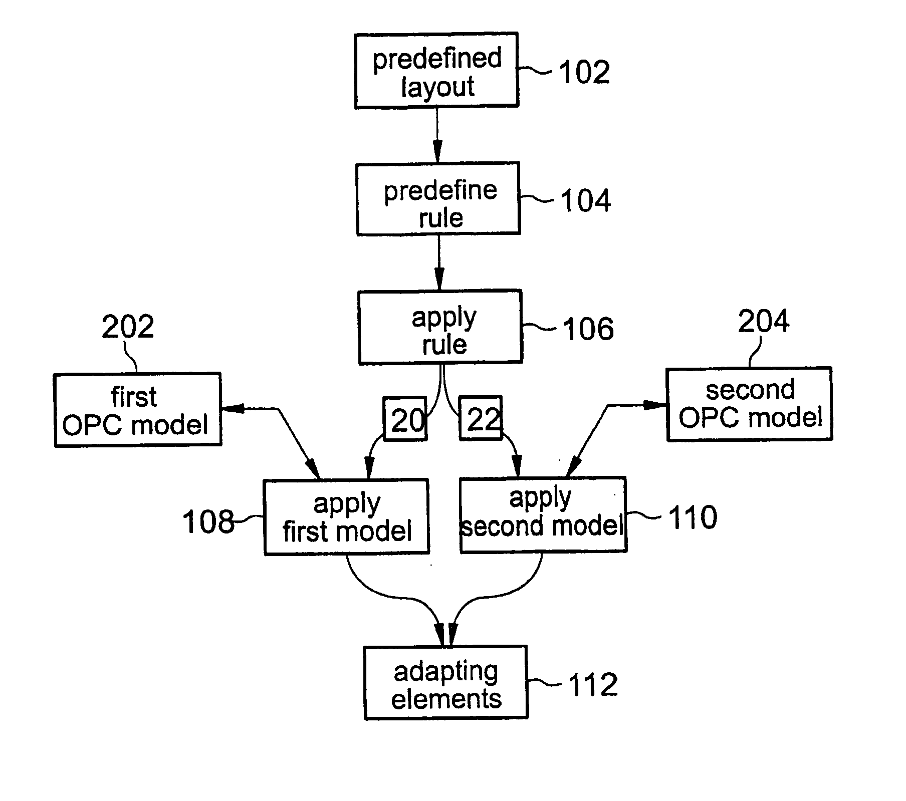
[0051]FIG. 1 shows, by way of example, the sequence of the method according to a preferred embodiment of the invention in a flow diagram. First, a layout for producing a mask plane is predefined (step 102). The layout has been extracted, for example, beforehand from the overall design of an integrated circuit.

[0052] The application of the further method is based on the knowledge that the concrete layout poses problems when projecting a mask onto a wafer. In particular, it has been found that the dimensions of the structures that have hitherto been OPC-corrected by means of...


PUM


Abstract

A respectively separate optical proximity correction (OPC) process model and method is formed for selected structure classes or partial patterns of a layout is disclosed. For this purpose, the corresponding structure elements are treated separately as early as during the modeling. During the modeling and also for OPC correction, the structure elements in the layout to be corrected are selected in correspondingly rule-based fashion. The thus selected elements of the layout are simulated and corrected with the separately formed OPC process models. The errors in the description of the imaging process are smaller for the separate OPC process models than for a uniform OPC process model, which has the effect of improving the accuracy of the imaging on the wafer in subsequent layout transfer processes.

Description

[0001] This application claims priority to German Patent Application 10 2005 003 001.7 which was filed Jan. 21, 2005, and is incorporated herein by reference. TECHNICAL FIELD [0002] The invention relates to methods for correcting the optical proximity effect when transferring patterns onto a substrate. BACKGROUND [0003] In the case of high integration densities or very small structure widths, for example in the region of the resolution limit of a projection system, imaging errors often occur when transferring structures from a mask onto a wafer. If the structure elements are particularly close together, then this may also result, in particular, in undesirable and unavoidable light contributions of respectively adjacent structure elements in the photosensitive layer. These proximity effects, also called proximity errors, may be caused by instances of light scattering or diffractions at chromium or other absorber edges on the mask, lens imperfections, varying resist thicknesses or mic...

Claims


Application Information

Patent Timeline
Patent Type & Authority Applications(United States)
IPC IPC(8): G06F17/50
CPCG03F1/144G03F1/36G03F7/70441
Inventor KECK, MARTIN
Owner QIMONDA
Why Eureka
Try Eureka