Laser processing method and laser beam processing machine

a laser beam processing machine and laser beam technology, applied in the direction of manufacturing tools, electrical/magnetic/electromagnetic heating, welding/soldering/cutting articles, etc., can solve the problems of difficult melt-divide only the adhesive film, the adhesive film for die bonding cannot be mounted on the back surface of the semiconductor wafer beforehand, and the bonding work cannot be smoothly carried ou

Inactive Publication Date: 2006-09-07
DISCO CORP
View PDF9 Cites 52 Cited by
  • Summary
  • Abstract
  • Description
  • Claims
  • Application Information

AI Technical Summary

Benefits of technology

[0011] It is an object of the present invention to provide a laser processing method and a laser beam processing machine capable of melt-dividing an adhesive film affixed to the back surface...

Problems solved by technology

According to the method disclosed by JP-A 2000-182995, however, when the adhesive film is cut together with the semiconductor wafer with the cutting blade to divide the semiconductor wafer into individual semiconductor chips, the back surfaces of the semiconductor chips may have chips or the adhesive film may have whisker-like burrs to cause disconnection at the time of wire bonding.
However, as when the semiconductor wafer is divided into individual semiconductor chips by the pre-dicing technique, after the dividing grooves having a predetermined depth are formed on the front surface of the semiconductor wafer along the streets, the back surface of the semiconductor wafer is ground to expose the dividing grooves to the back surface, the adhesive film for die bonding cannot be mounted on the back surface of the semiconductor wafer beforehand.
Accordingly, to bond the semiconductor chips to the die bonding frame for supporting the semiconductor chips in the pre-dicing technique, a bonding agent must be inserted between the semiconductor chips and the die bonding frame, thereby making it impossible to carry out the bonding work smoothly.
Howe...

Method used


Image

  • Laser processing method and laser beam processing machine
  • Laser processing method and laser beam processing machine
  • Laser processing method and laser beam processing machine

Examples


Embodiment Construction

[0041] Preferred embodiments of the laser processing method and the laser beam processing machine of the present invention will be described in detail hereinunder with reference to the accompanying drawings.

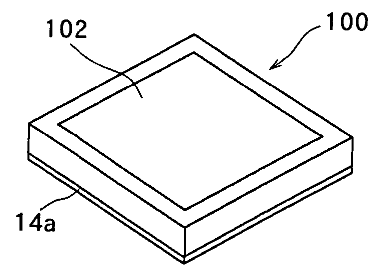
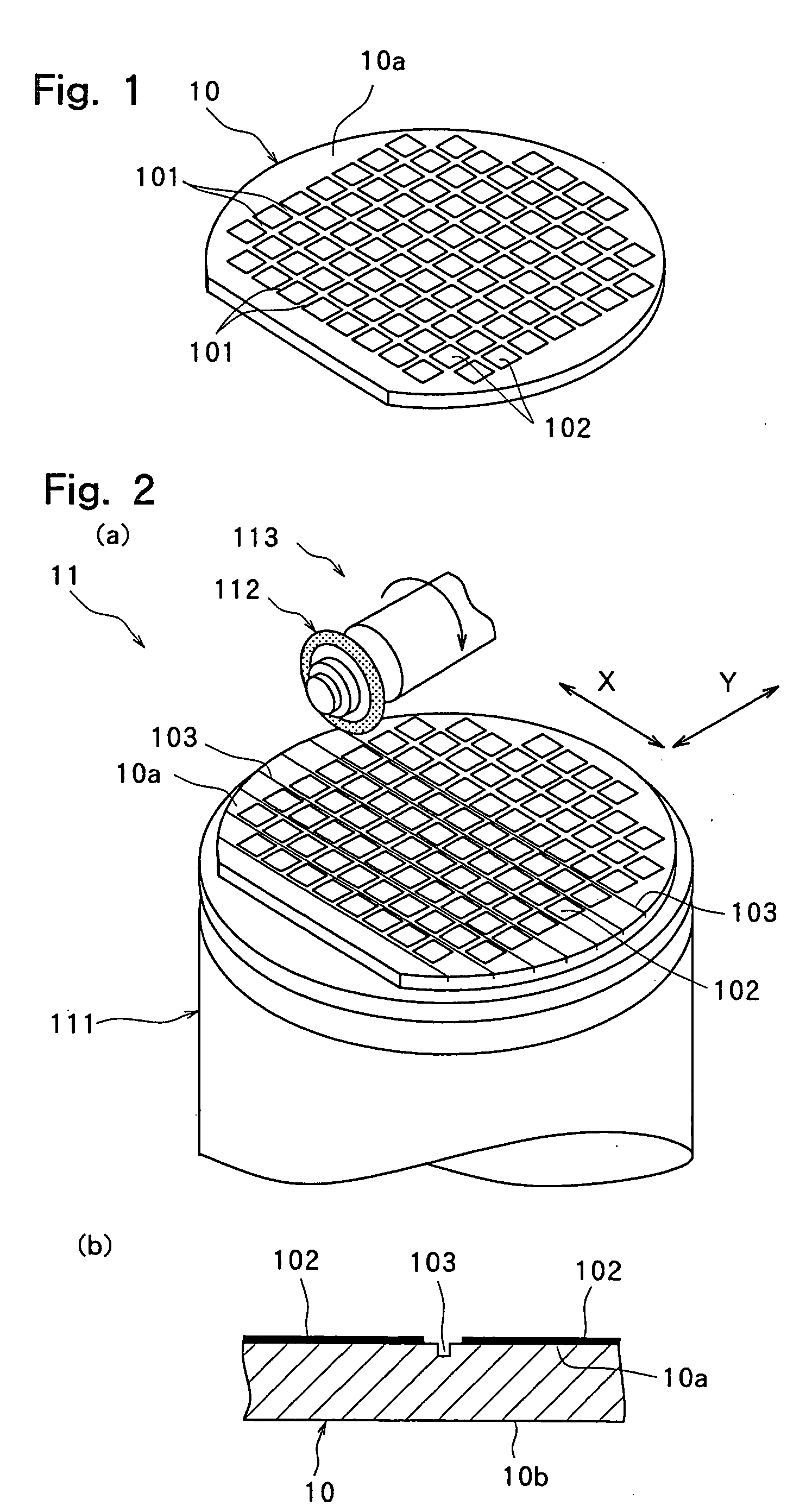
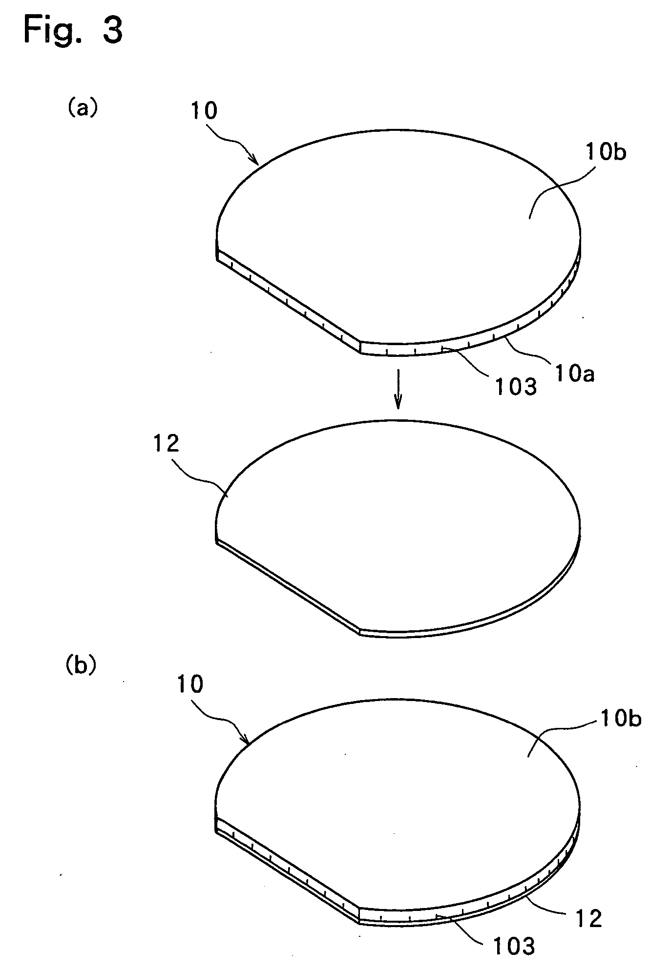
[0042]FIG. 1 is a perspective view of a semiconductor wafer to be divided into a plurality of semiconductor chips. The semiconductor wafer 10 shown in FIG. 1 is, for example, a silicon wafer having a thickness of 600 μm, a plurality of streets 101 are formed in a lattice pattern on the front surface 10a, and a device 102 is formed in each of a plurality of areas sectioned by the plurality of streets 101. The process for manufacturing semiconductor chips by dividing this semiconductor wafer 10 into individual semiconductor chips will be described hereinunder.

[0043] To divide the semiconductor wafer 10 into individual semiconductor chips, dividing grooves having a predetermined depth (corresponding to the final thickness of each semiconductor chip) are first formed along the stre...


PUM

PropertyMeasurementUnit
Widthaaaaaaaaaa

Abstract

A laser processing method for melt-dividing an adhesive film for die bonding affixed to the back surface of a semiconductor wafer which has been separated into a plurality of semiconductor chips and which is put on an extensible dicing tape mounted on an annular frame along dividing grooves for separating the plurality of semiconductor chips from one another, comprising the steps of a tape expanding step for expanding the dicing tape affixed to the semiconductor wafer to increase the width of the dividing grooves for separating the plurality of semiconductor chips from one another; and an adhesive film melt-dividing step for melt-dividing the adhesive film along the dividing grooves by applying a laser beam to the adhesive film along the dividing grooves in a state where the width of the dividing grooves for separating the plurality of semiconductor chips from one another has been increased.

Description

FIELD OF THE INVENTION [0001] The present invention relates to a laser processing method for melt-dividing an adhesive film for die bonding, which is affixed to the back surface of a semiconductor wafer that has been separated into a plurality of semiconductor chips, and to a laser beam processing machine. DESCRIPTION OF THE PRIOR ART [0002] In the manufacturing process of a semiconductor device, for example, individual semiconductor chips are manufactured by forming a device such as IC or LSI in a plurality of areas sectioned by streets (cutting lines) formed in a lattice pattern on the front surface of a substantially disk-like semiconductor wafer and dividing the semiconductor wafer into the areas having device formed thereon, along the streets. A dicing machine is generally used as the dividing machine for dividing the semiconductor wafer to cut the semiconductor wafer along the streets with a cutting blade having a thickness of about 20 μm. The thus obtained semiconductor chips...

Claims


Application Information

Patent Timeline
IPC IPC(8): H01L21/78H05B6/00
CPCB23K26/10B23K26/4065H01L21/6835H01L21/6836H01L21/78H01L24/27H01L24/83H01L2221/68327H01L2221/68336H01L2224/83191H01L2224/8385H01L2924/01005H01L2924/01013H01L2924/01015H01L2924/01074H01L2924/07802H01L2224/2919H01L2924/01006H01L2924/01019H01L2924/01033H01L2924/0665H01L2924/00H01L24/29H01L2924/3512B23K2103/42B23K2103/50
Inventor YOSHIKAWA, TOSHIYUKISHIGEMATSU, KOICHI
Owner DISCO CORP
Why Eureka
Try Eureka