Variable gain wideband amplifier

a wideband amplifier and variable gain technology, applied in the direction of gain control, positive-feedback circuit arrangement, amplification control device circuit, etc., can solve the problems of poor linearity, worse noise characteristics of the transistor on the feedback path,

Inactive Publication Date: 2006-09-07
SAMSUNG ELECTRO MECHANICS CO LTD
View PDF6 Cites 5 Cited by
  • Summary
  • Abstract
  • Description
  • Claims
  • Application Information

AI Technical Summary

Benefits of technology

[0024] In this case, the load circuit may further comprise a third field effect transistor having a drain connected to the output signal terminal, a source connected to the drain of the main field effect transistor of the inversion amplifier circuit and a gate connected to third control voltage, in which the third control voltage may have a preset magnitude of constant voltage.
[0025] Preferably, the load circuit may further comprise a fourth field effect transistor a drain connected to one end of the load circuit, a source connected to the other end of the lo

Problems solved by technology

Since the active device has its own resistance, there is a problem in that the FET transistor on the feedback path worsens noise characteristics.
Then, such third or

Method used


Image

  • Variable gain wideband amplifier
  • Variable gain wideband amplifier
  • Variable gain wideband amplifier

Examples


Embodiment Construction

[0035] A preferred embodiment of the present invention will now be described in detail with reference to the accompanying drawings, in which the same reference signs are used to designate the same or reference components throughout.

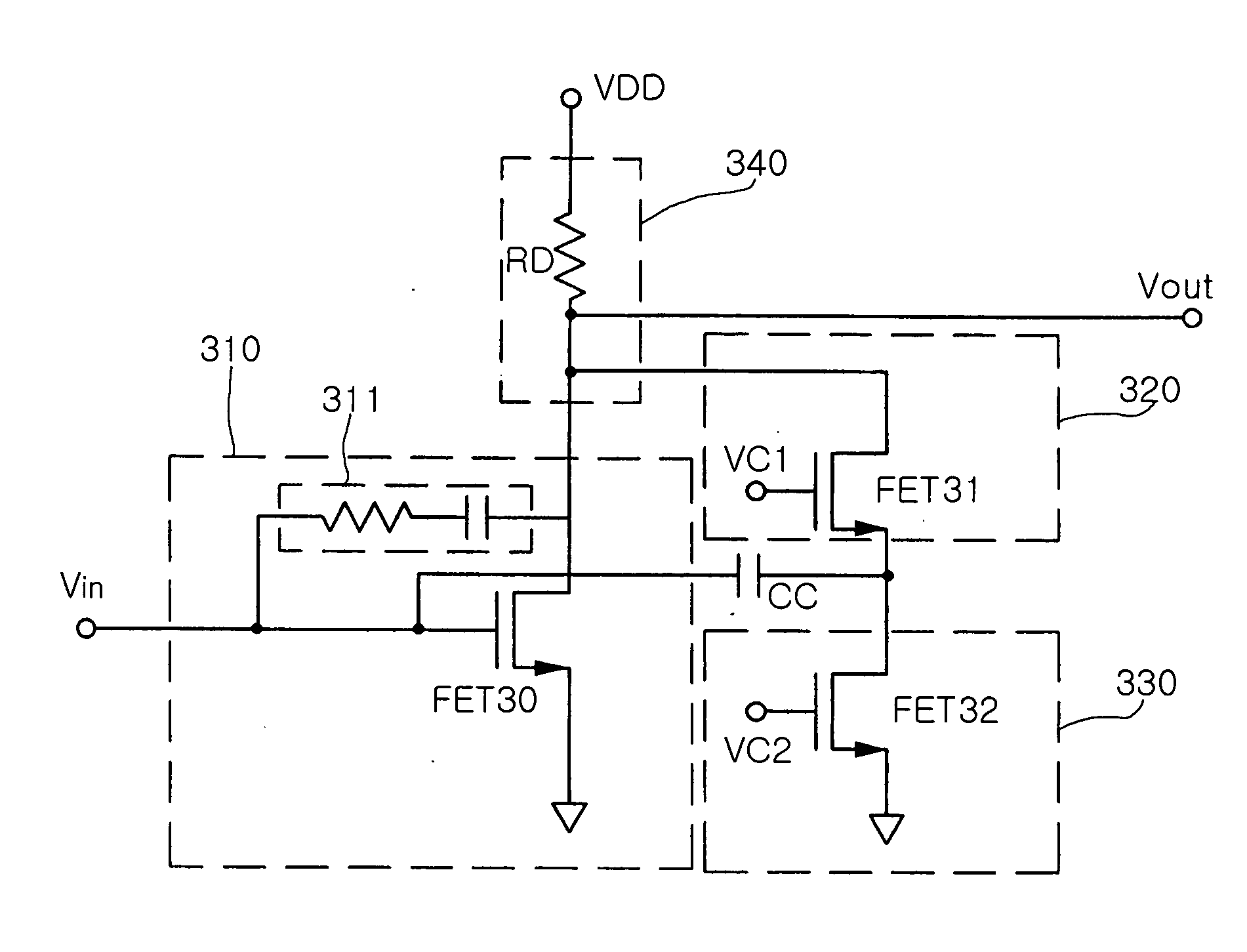
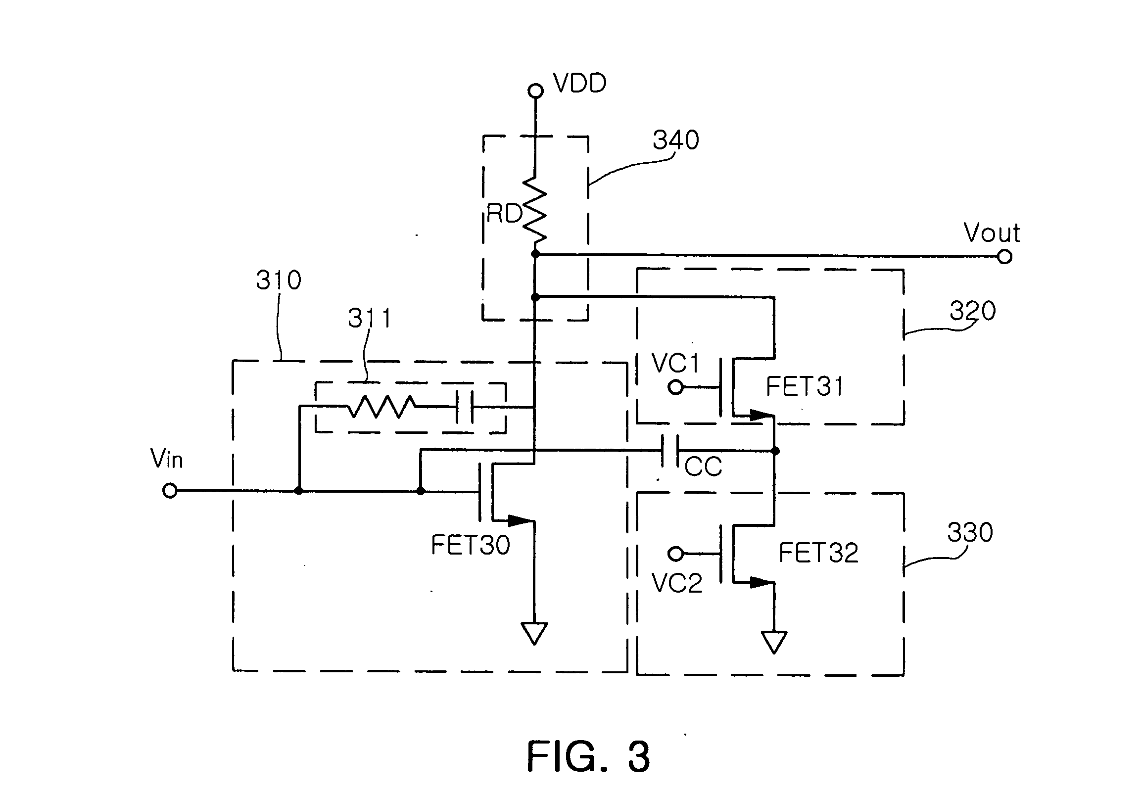
[0036]FIG. 3 is a circuit diagram illustrating a variable gain wideband amplifier of the invention. Referring to FIG. 3, the variable gain wideband amplifier includes a feedback-type inversion amplifier circuit 310 for amplifying input Vin, a feedback-type non-inversion amplifier circuit 320 for amplifying input Vin, a power source circuit 330 for controlling the gain of the non-inversion amplifier circuit 320 and a load circuit 340 connected between a junction of output terminals of the inversion and non-inversion amplifier circuits 310 and 320 and power voltage potential VDD to control the gain of the amplifier circuits 310 and 320.

[0037] The variable gain wideband amplifier of the invention is feedforward type, which can output signals from the inver...


PUM


Abstract

The invention relates to a feedback or feedforward type variable gain wideband amplifier. The variable gain wideband amplifier includes a feedback-type inversion amplifier circuit 310 for amplifying input Vin, a feedback-type non-inversion amplifier circuit 320 for amplifying input Vin, a power source circuit 330 for controlling the gain of the non-inversion amplifier circuit 320 and a load circuit 340 connected between a junction of output terminals of the inversion and non-inversion amplifier circuits 310 and 320 and power voltage potential VDD to control the gain of the amplifier circuits 310 and 320. The variable gain wideband amplifier of the invention is feedforward type, and outputs signals from the inversion and non-inversion amplifier circuits 310 and 320 via a single output terminal in order to attenuate third order intermodulation frequency IM3 generated from the amplifier circuits 310 and 320. Then, predetermined frequencies f1 and f2 included in the input signal are amplified.

Description

RELATED APPLICATION [0001] The present application is based on and claims priority from Korean Application Number 2005-17434, filed Mar. 2, 2005, the disclosure of which is hereby incorporated by reference herein in its entirety. BACKGROUND OF THE INVENTION [0002] 1. Field of the Invention [0003] The present invention relates to a variable gain wideband amplifier to be used as a low noise amplifier in a wideband system. More particularly, the invention relates to a feedback or feedforward type variable gain wideband amplifier. [0004] 2. Description of the Related Art [0005] Currently, communication systems are required to operate at least two different frequency channels owing to increasing multiband implementation. When applied to a communication system using different frequency channels, an amplifier has to amplify different frequency channels in wideband. In addition, since all existing amplifiers have nonlinear characteristics, it is required to provide means for reducing third ...

Claims


Application Information

Patent Timeline
IPC IPC(8): H03G3/30
CPCH03F1/223H03F1/3205H03F1/342H03F3/193H03F3/345H03F2200/117H03F2200/141H03F2200/372H03G1/007H03G1/0088H03G3/10H03G3/30H03F1/34
Inventor KIM, MOON SUNBAEK, WON JIN
Owner SAMSUNG ELECTRO MECHANICS CO LTD
Why Eureka
Try Eureka