Embedded multilayer chip capacitor and printed circuit board having the same

Active Publication Date: 2006-09-07
SAMSUNG ELECTRO MECHANICS CO LTD
View PDF9 Cites 55 Cited by
  • Summary
  • Abstract
  • Description
  • Claims
  • Application Information

AI Technical Summary

Benefits of technology

[0030] The upper and lower terminals of the multilayer chip capacitors arranged horizontally are directly connected to respective top and bottom conductive layers formed on the printed circuit board. This eliminates a need for via h

Problems solved by technology

With higher density and integration of electronic circuits, printed circuit boards lack a space for mounting a passive device.
The chipping or cracking undermines reliability of the capacitor and possibly causes malfunction thereof.
This laser process increases manufacturing costs of the printed circuit board significantly.
Also, smaller size in the multilayer chi

Method used


Image

  • Embedded multilayer chip capacitor and printed circuit board having the same
  • Embedded multilayer chip capacitor and printed circuit board having the same
  • Embedded multilayer chip capacitor and printed circuit board having the same

Examples


Embodiment Construction

[0045] The present invention now will be described more fully hereinafter with reference to the accompanying drawings, in which preferred embodiments of the invention are shown. This invention may, however, be embodied in many different forms and should not be construed as limited to the embodiments set forth herein. Rather, these embodiments are provided so that this disclosure will be thorough and complete, and will fully convey the scope of the invention to those skilled in the art. In the drawings, the thickness of layers and regions are exaggerated for clarity.

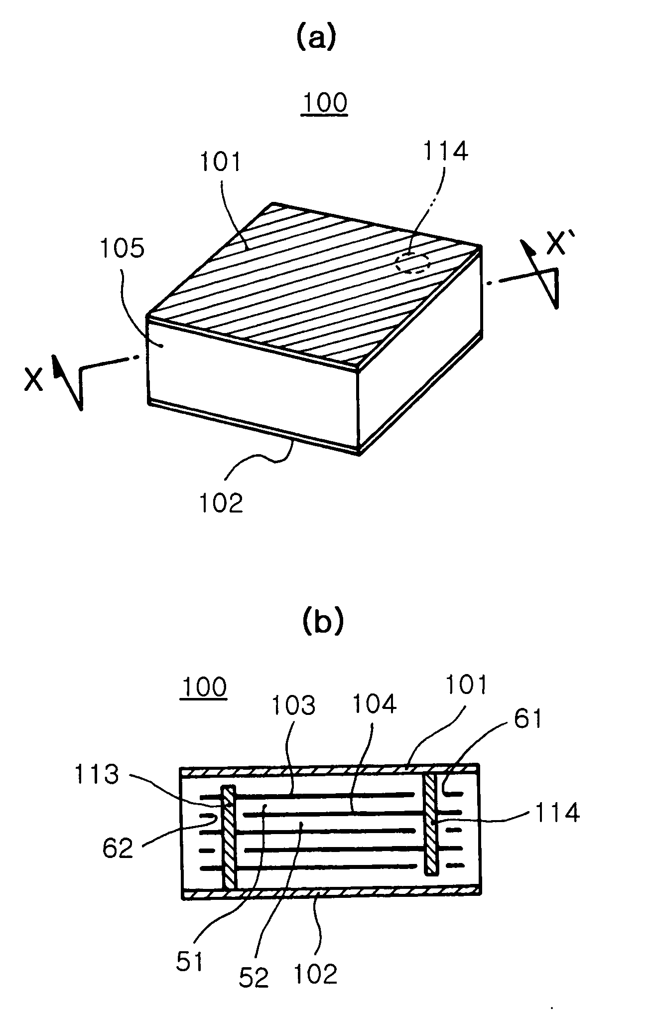
[0046]FIG. 3(a) is a fragmentary perspective view of an embodiment of an embedded multilayer chip capacitor according to the invention, and FIG. 3(b) is a sectional view of the capacitor taken along the line XX′ in FIG. 3(a). Referring to FIGS. 3(a) and 3(b), an embedded multilayer chip capacitor 100 of the invention includes a capacitor body 105, an upper external electrode 101 formed on a top of the capacitor body 105,...


PUM

PropertyMeasurementUnit
Lengthaaaaaaaaaa
Lengthaaaaaaaaaa
Diameteraaaaaaaaaa

Abstract

The invention provides an embedded multilayer chip capacitor, and a printed circuit board having the same. The embedded multilayer chip capacitor comprises a capacitor body having a plurality of dielectric layers stacked one on another; a plurality of first and second internal electrodes formed inside the capacitor body, separated by the dielectric layers; and first and second vias extended vertically inside the capacitor body. The first via is connected to the first internal electrodes and the second via is connected to the second internal electrodes. The first via is led to a bottom of the capacitor body and the second via is led to a top of the capacitor body.

Description

RELATED APPLICATION [0001] This application claims the benefit of Korean Patent Application No. 2005-0018702 filed on Mar. 7, 2005, in the Korean Intellectual Property Office, the disclosure of which is incorporated herein by reference. BACKGROUND OF THE INVENTION [0002] 1. Field of the Invention [0003] The present invention relates to a multilayer chip capacitor. More particularly, the present invention relates to a highly-reliable embedded multilayer chip capacitor, and a printed circuit board having the same. [0004] 2. Description of the Related Art [0005] With higher density and integration of electronic circuits, printed circuit boards lack a space for mounting a passive device. To overcome this, efforts have been under way to implement embedded devices or parts embedded in the board. Especially, various suggestions have been made regarding a method for embedding a capacitor, used as capacitive parts, in the board. In a method to embed the capacitor in the board, the board itse...

Claims


Application Information

Patent Timeline
IPC IPC(8): H01G4/228
CPCH01G2/06H01G4/232H01G4/30H05K1/0231H01L2924/0002H05K2201/10643H05K1/185H01L2924/00H01G4/12
Inventor SHIM, CHANG HOONAN, JIN YONGCHO, SUK HYEONKANG, SUNG HYUNG
Owner SAMSUNG ELECTRO MECHANICS CO LTD
Why Eureka
Try Eureka