Contact-type monolithic image sensor

a monolithic optical image and contact-type technology, applied in the field of monolithic optical image sensors, can solve the problems of increasing the number of problems that remain unsolved, reducing the resolution capacity of conventional bar-code readers, and being relatively expensive devices. the effect of thickness reduction

Inactive Publication Date: 2006-09-14
MICROALIGN TECH
View PDF4 Cites 35 Cited by
  • Summary
  • Abstract
  • Description
  • Claims
  • Application Information

AI Technical Summary

Benefits of technology

[0025] It can be summarized that, although the system described in the aforementioned international patent application, as well in other references are good examples of the current trend to miniaturization of image-forming and image-receiving packages, the aforementioned trend is limited by complexity of manufacturing and assembling, as well as by the lack of standardized elements and sub-assemblies that otherwise could be used for assembling systems different in their purposes.
[0026] It is an object of the invention to provide a thin flat monolithic image sensor that has a thickness reduced to the dimension unattainable in conventional flat image sensors. It is another object to provide a thin flat monolithic image sensor having a thin-layered laminated structure that consists of an optical layer and an image-receiving layer, wherein the optical layer incorporates a light source for illumination of the sensor's surface that is in contact with an object the image of which is to be reproduced. It is another object to provide the flat monolithic sensor, wherein the aforementioned thin-layered laminated structure is assembled fr

Problems solved by technology

In spite of the recent progress in the field of machine vision and image sensing, a number of problems still remain unsolved.
This is because conventional bar-code readers have a limited resolution capacity.
Such an objective may be a rather bulky and relatively expensive device that will make the entire image-sensing device 20 large and expensive.
It is obvious that the lack of direct illumination of the finger surface significantly lowers image-recognition capacity of the device.
For example, such a device cannot reproduce an image on the flat surface of the object, e.g., a signature written on a flat card, etc.
In spite of the fact that the idea of compacting the sensing and image-receiving flat and thin elements into a monolithic sensor is rather attractive, such known devices as shown in FIG. 3 did not find commercial application in view of disadvantages inherent in these devices.
However, in spite of great miniaturization, images produced by the aforementioned device are not comparable in quality, e.g., with FTIR images.
However, none of these n

Method used


Image

  • Contact-type monolithic image sensor
  • Contact-type monolithic image sensor
  • Contact-type monolithic image sensor

Examples


Embodiment Construction

—PREFERRED EMBODIMENTS—FIGS. 5-16

General Features of Two Embodiments

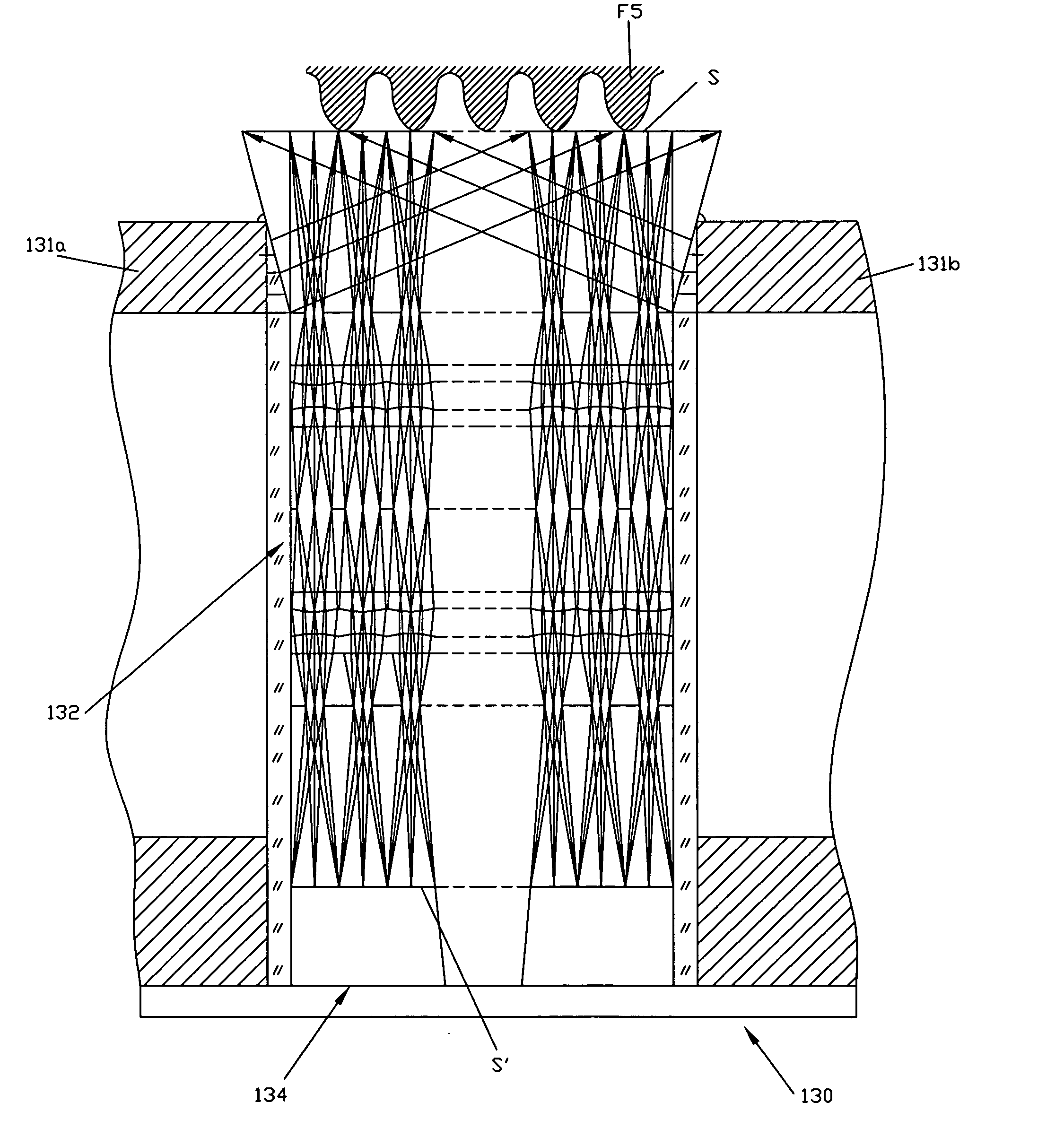
[0135] In general, the sensor of the invention can be realized in two different embodiments. Although the principle of the invention is common for both embodiments, each embodiment can be realized in several slightly different modifications. In one preferred embodiment of a sensor 120a, a schematic sectional view of which is shown in FIG. 5, a light source (sources) 122a is (are) located on the lateral side (sides) of the optical layer for illuminating the inner top surface of the glass plate which is in contact with the object. In the second preferred embodiment of a sensor 120b, which is schematically shown in cross section in FIG. 6, an interlayer light source 122b is made in the form of a single or a multiple light-emitting diode source embedded into the laminated optical layer. The subsequent description of parts and elements that are identical in both sensors 120a and 120b (FIG. 5 and FIG. 6) will be related...


PUM


Abstract

A thin monolithic image sensor of the invention is comprised of a laminated solid package composed essentially of an optical layer and an image-receiving layer placed on the top of the optical layer. The optical layer also comprises a laminated structure composed of at least an optical microlens-array sublayer and an aperture-array sublayer. The image-receiving layer is a thin flat CCD/CMOS structure that may have a thickness of less than 1 mm. The image digitized by the CCD/CMOS structure of the sensor can be transmitted from the output of the image-receiving layer to a CPU for subsequent processing and, if necessary, for displaying. A distinguishing feature of the sensor of the invention is that the entire sensor along with a light source has a monolithic structure, and that the diaphragm arrays are located in planes different from the plane of the microlens array and provide the most efficient protection against overlapping of images produced by neighboring microlenses.

Description

CROSS-REFERENCE TO RELATED APPLICATIONS [0001] not applicable FEDERALLY SPPONSORED RESEARCH [0002] not applicable SEQUENCE LISTING OF PROGRAM [0003] not applicable BACKGROUND OF THE INVENTION—FIELD OF INVENTION [0004] The present invention relates to monolithic optical image sensors, in particular to contact-type monolithic optical image sensors for precision measurement of configurations, shapes, and dimensions of flat objects or flat parts of the objects that are in contact with the aforementioned sensors. The image sensors of the invention may find use in the manufacture of miniature and precision parts, for sorting precision parts, as well as for identification of various parts and objects in open, as well as in hard-to-get areas, such as thin slots, e.g., of banking automatic teller machines. Another possible application is for security purposes, e.g., identification of biometric images, such as fingerprints, signatures, or the like, in combination with coded data. BACKGROUND O...

Claims


Application Information

Patent Timeline
IPC IPC(8): H01L27/00
CPCH01L27/14678G06K9/0004G06V40/1318
Inventor GUREVICH, IGORFAYBISHENKO, VICTORVELIKOV, LEONID
Owner MICROALIGN TECH
Why Eureka
Try Eureka