

Electron emission device and method for manufacturing the same
a technology of electron beam and emission device, which is applied in the manufacture of electrode systems, electric discharge tubes/lamps, and discharge tubes luminescnet screens, etc., can solve the problems of deteriorating deteriorating screen color purity, and difficulty in wet etching process to form opening portions with a high vertical to horizontal ratio, etc., to achieve high resolution screen image and enhance electron beam focusing efficiency
- Summary
- Abstract
- Description
- Claims
- Application Information
AI Technical Summary
Benefits of technology
Problems solved by technology
Method used
Image

Examples
Embodiment Construction
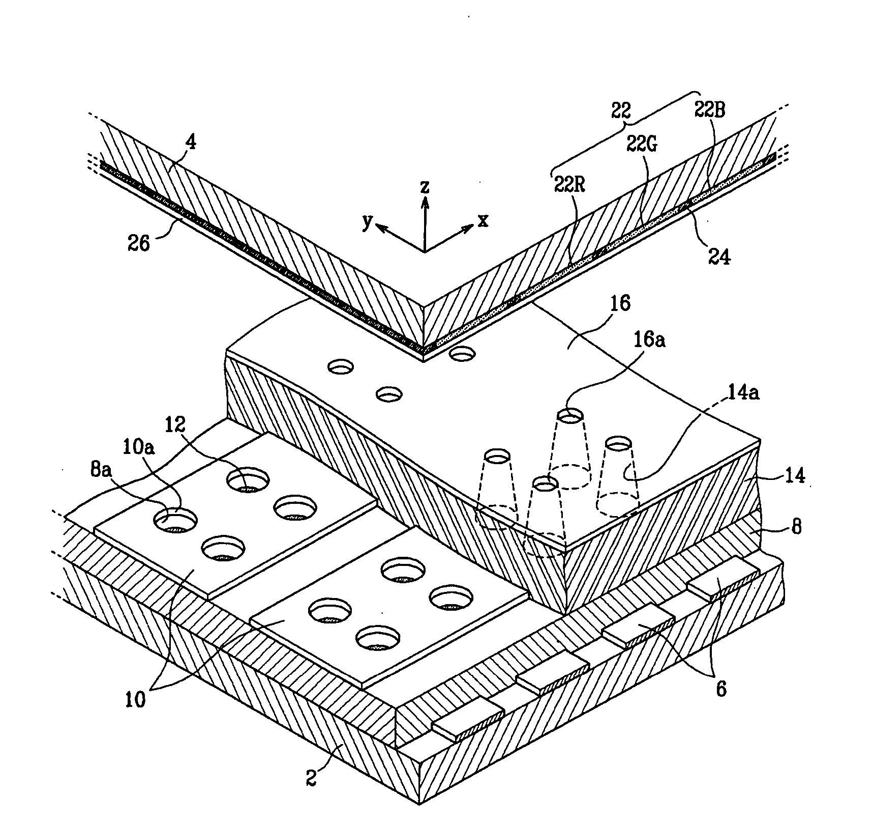
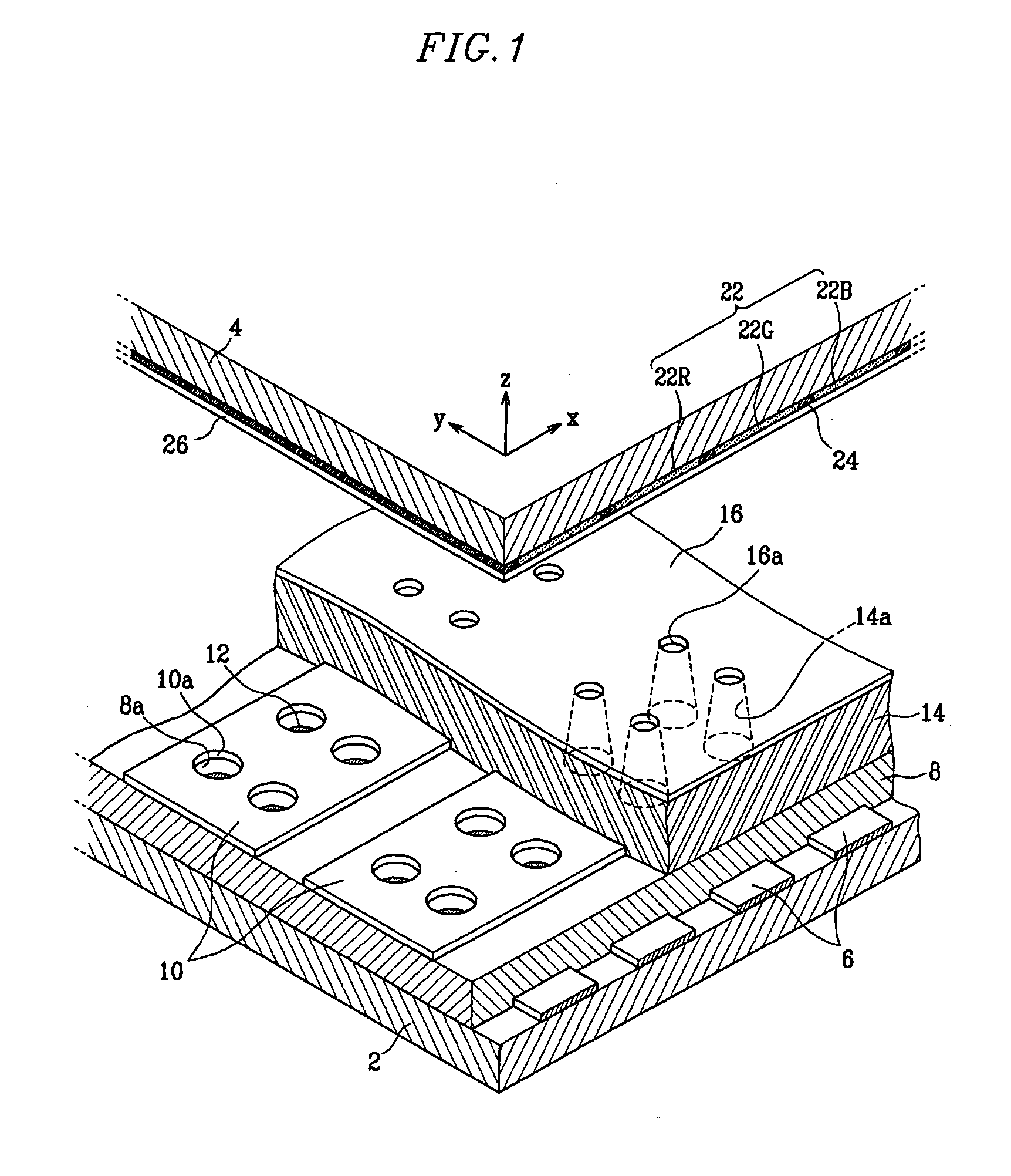
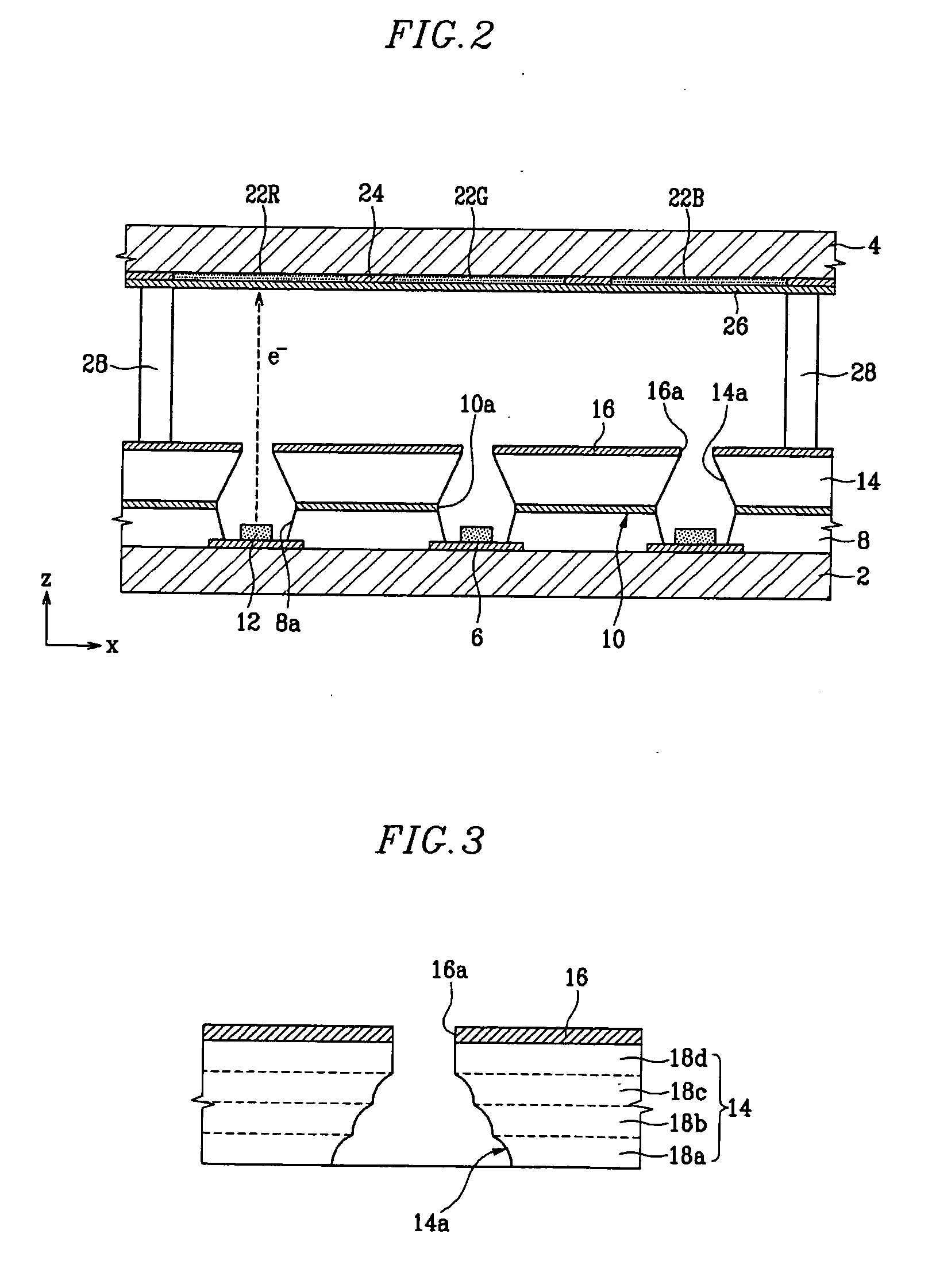
[0025] Referring now to FIGS. 1 and 2, the electron emission device includes first and second substrates 2, 4 arranged substantially parallel to each other with an inner space therebetween. An electron emission structure is provided at the first substrate 2 to emit electrons, and a light emission or display structure is provided at the second substrate 4 to emit visible light rays due to the electrons.
[0026] Specifically, cathode electrodes 6 are stripe-patterned on the first substrate 2 in a direction of the first substrate 2 (in the y axis direction). A first insulating layer 8 is formed on the entire surface of the first substrate 2 while covering the cathode electrodes 6. Gate electrodes 10 are stripe-patterned on the first insulating layer 8 while proceeding substantially perpendicular to the cathode electrodes 6 (in the x axis direction).
[0027] When the crossed regions of the cathode and the gate electrodes 6, 10 are defined as the pixel regions, at least one electron emissi...
PUM
 Abstract
Description
Claims
Application Information