Solid-state imaging device and camera

a solid-state imaging and camera technology, applied in the field of solid-state imaging devices and cameras, can solve the problems of deterioration of signal-to-noise ratio, decrease of output per pixel, and degradation of pixel characteristics, so as to improve the range of output signals, increase the amount of saturation charges, and improve the sensitivity of luminosity signals.

Inactive Publication Date: 2009-08-27
SONY SEMICON SOLUTIONS CORP
View PDF6 Cites 46 Cited by
  • Summary
  • Abstract
  • Description
  • Claims
  • Application Information

AI Technical Summary

Benefits of technology

[0015]The solid-state imaging device according to an embodiment of the invention includes at least the white photoelectric conversion element and the light-shielded diode element, and both of the elements are connected with each other by way of an overflow path. With the present structure of the solid-state imaging device, upon the incidence of high intensity light to the white photoelectric conversion element, the charges overflowed from the white photoelectric conversion element enter into and are accumulated in the light-shielded diode element. As a result, the saturation charges of the white photoelectric conversion element amount to the sum of the amount accumulated in the white photoelectric conversion element and the light-shielded diode element. On the other hand, in each of the color photoelectric conversion elements, the charges can properly be accumulated so as to yield the nominal output level of signals for the photoelectric conversion elements.
[0016]With the solid-state imaging device according to an embodiment of the present invention, the luminosity signal sensitivity can be improved by increasing the amount of saturation charges of the white photoelectric conversion element. In addition, the output signal range is improved for each of the color photoelectric conversion elements. With the camera according to an embodiment of the present invention, high sensitivity and high power picture images can be obtained by incorporating the solid-state imaging device mentioned as above.

Problems solved by technology

In the solid-state imaging device, the reduction of a pixel size may cause the degradation of pixel characteristics.
That is, the output per a pixel decreases and the signal-to-noise ratio deteriorates.
However, in regard to purely optical characteristics such as the abovementioned sensitivity, the trend of degradation including color mixing is proceeding at an accelerating pace with an additional difficulty in proper light condensation.
For an image sensor having a relatively low working voltage such as the CMOS image sensor, the depletion potential of the photodiode is relatively shallow and the amount of charge accumulation is not sufficiently large.
Therefore, even if the luminosity signal sensitivity of the white pixel is increased, the amount of light can only be handled at most to the extent not to saturate the white pixel photodiode.

Method used


Image

  • Solid-state imaging device and camera
  • Solid-state imaging device and camera
  • Solid-state imaging device and camera

Examples


first embodiment

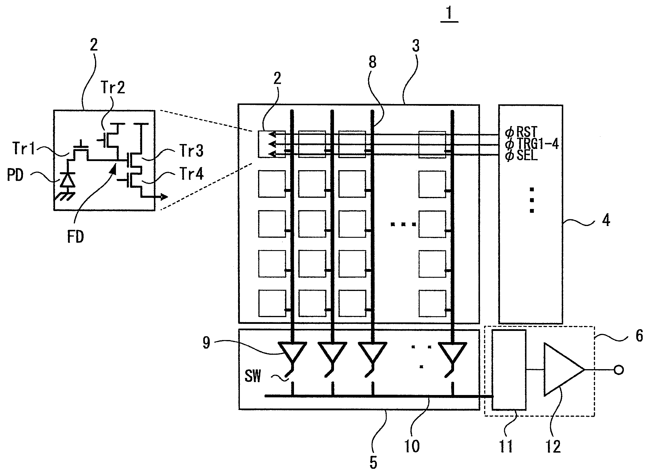
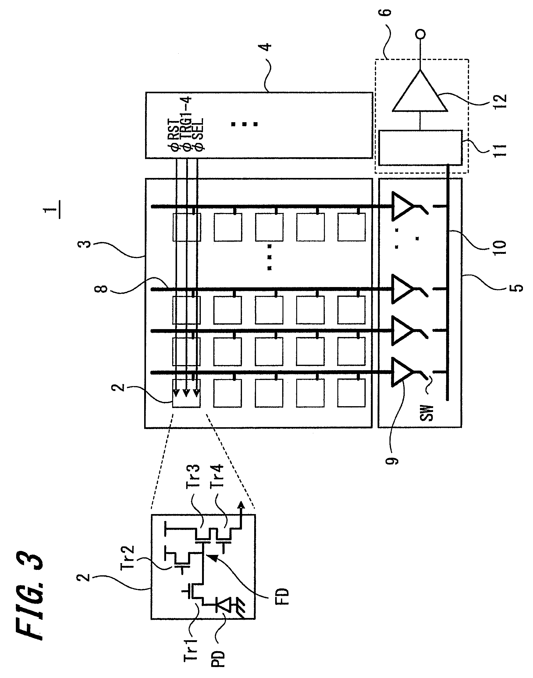
[0053]FIG. 4 is a schematic view illustrating the major portion of an imaging section included in the solid-state imaging device, according to the present invention. This drawing illustrates diagrammatically the configuration of pixels in the imaging section, particularly the arrangement configuration of photodiodes serving as photoelectric conversion elements constituting the pixels. In the present embodiment, the photoelectric conversion elements include a group of photodiodes including color photodiodes PD configured to convert light signals in respective wavelength ranges of as red (R), green (G), and blue (B) to electric signals (hereinafter referred to as a red photodiode PDr, a green photodiode PDg, and a blue photodiode PDb, respectively); another photodiode PD configured to convert to further electric signals from light signals in the wavelength range including the entire visible light range and a portion of the infrared light range (hereinafter referred to as a white photo...

fourth embodiment

[0076]Into the structure of the fourth embodiment, the aforementioned inner lens and waveguide structure shown in FIGS. 9 and 10 respectively may also be incorporated.

[0077]FIG. 14 is a drawing generally illustrating a configuration adapted to a solid-state imaging device or CMOS image sensor according to another embodiment of the present invention. The solid-state imaging device of the present embodiment is provided by arranging a plurality of sets in which pixel transistors other than the transfer transistor are shared by a plurality of pixels each provided with photodiodes as photoelectric conversion elements, in this example, four pixels provided with four photodiodes (the set being hereinafter referred to as a sharing pixel).

[0078]The solid-state imaging device 51 according to the present embodiment includes an imaging section 3 (so-called pixel section) in which a plurality of sharing pixels 52 are arranged in a two-dimensional array, and peripheral circuits disposed around th...

fifth embodiment

[0082]In addition, FIGS. 15A, 15B, and 15C are schematic views illustrating the planar configuration of the sharing pixel 52 according to the invention. One set of the sharing pixel 52 according to the present embodiment includes two pixels each vertically and horizontally, four pixels in total. This one set as the sharing pixel 52 corresponds to the aforementioned unit of FIGS. 4, 5A, 5B, and 5C, and the sharing pixel includes one color photodiode PDc out of red, green, and blue color photodiodes, one white photodiode PDw, and two light-shielded diodes Dls (Dls1, Dls2).

[0083]In this embodiment, as shown in FIG. 15A, a common floating diffusion region (FD) 54 is disposed at the center of the structure so as to be shared. The photodiodes PDw, PDc and diodes Dls1, Dls2 are disposed in the two-by-two arrangement, i.e., two of them horizontally and two vertically, so as to hold the common floating diffusion region (FD) 54 in the middle of the structure. Each transfer gate electrode 55 (...


PUM


Abstract

Disclosed is a solid-state imaging device which includes a group of elements, the group including at least color photoelectric conversion elements configured to convert light signals in first, second, and third wavelength ranges to electric signals, respectively, a white photoelectric conversion element configured to convert light signals in the wavelength range including the entire visible light range and a portion of the infrared light range to electric signals, and a light-shielded diode element configured to be shielded from light. A unit is formed by including the white photoelectric conversion element and the light-shielded diode element for one color photoelectric conversion element, and within the unit, the white photoelectric conversion element is electrically connected with the light-shielded diode element by way of an overflow path. A camera provided with the solid-state imaging device is also disclosed.

Description

CROSS REFERENCES TO RELATED APPLICATIONS[0001]The present invention contains subject matter related to Japanese Patent Application JP 2008-045213 filed in the Japanese Patent Office on Feb. 26, 2008, the entire contents of which being incorporated herein by reference.BACKGROUND OF THE INVENTION[0002]1. Field of the Invention[0003]The invention generally relates to solid-state imaging devices and cameras. More particularly, the invention relates to a solid-state imaging device and a camera provided with the solid-state imaging device.[0004]2. Description of the Related Art[0005]Solid-state imaging devices are classified broadly into amplification type solid-state imaging devices, which are typically illustrated by CMOS (complementary metal-oxide semiconductor) image sensors, and charge transfer type imaging devices, which are typified by CCD (charge-coupled device) image sensors.[0006]As to CMOS image sensors, the trend of replacement has been in progress at rapid speed particularly ...

Claims


Application Information

Patent Timeline
Patent Type & Authority Applications(United States)
IPC IPC(8): H04N5/335H04N5/225H01L27/14H01L27/146H04N5/355H04N5/369H04N5/374
CPCH01L27/14603H01L27/1463H01L27/14625H04N25/48H04N25/57H04N25/76
Inventor KUDOH, YOSHIHARU
Owner SONY SEMICON SOLUTIONS CORP
Why Eureka
Try Eureka