Semiconductor device and manufacturing process therefor

a technology of semiconductor devices and manufacturing processes, applied in semiconductor devices, semiconductor/solid-state device details, electrical apparatus, etc., can solve the problems of defective burying of vias, poor yield and unstability of semiconductor devices,

Active Publication Date: 2006-09-21
RENESAS ELECTRONICS CORP
View PDF6 Cites 36 Cited by
  • Summary
  • Abstract
  • Description
  • Claims
  • Application Information

AI Technical Summary

Benefits of technology

[0036] As described above, a connection resistance between the plug and the interconnect and a dielectric constant of the insulating film can be effectively reduced in accordance with the present invention.

Problems solved by technology

However, when forming an interconnect or connection plug made of Cu by dual damascene process, a semiconductor device is manufactured in a poor yield and unstably.
However, our investigation of the process has demonstrated that a removed material from the bottom may adhere to, for example, a sidewall of the contact hole, leading to insufficient removal.
Thus, a barrier metal film may not be stably formed in the contact hole, leading to problems such as defective burying of a via.

Method used


Image

  • Semiconductor device and manufacturing process therefor
  • Semiconductor device and manufacturing process therefor
  • Semiconductor device and manufacturing process therefor

Examples


embodiment 1

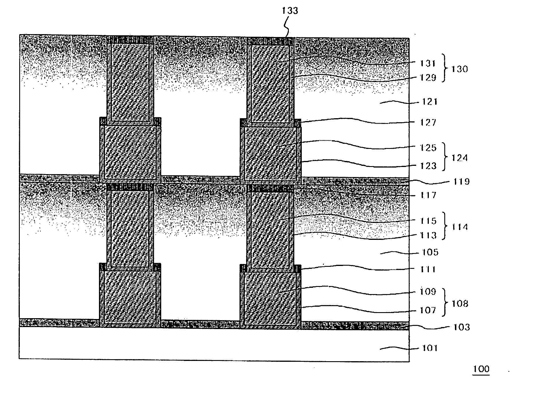
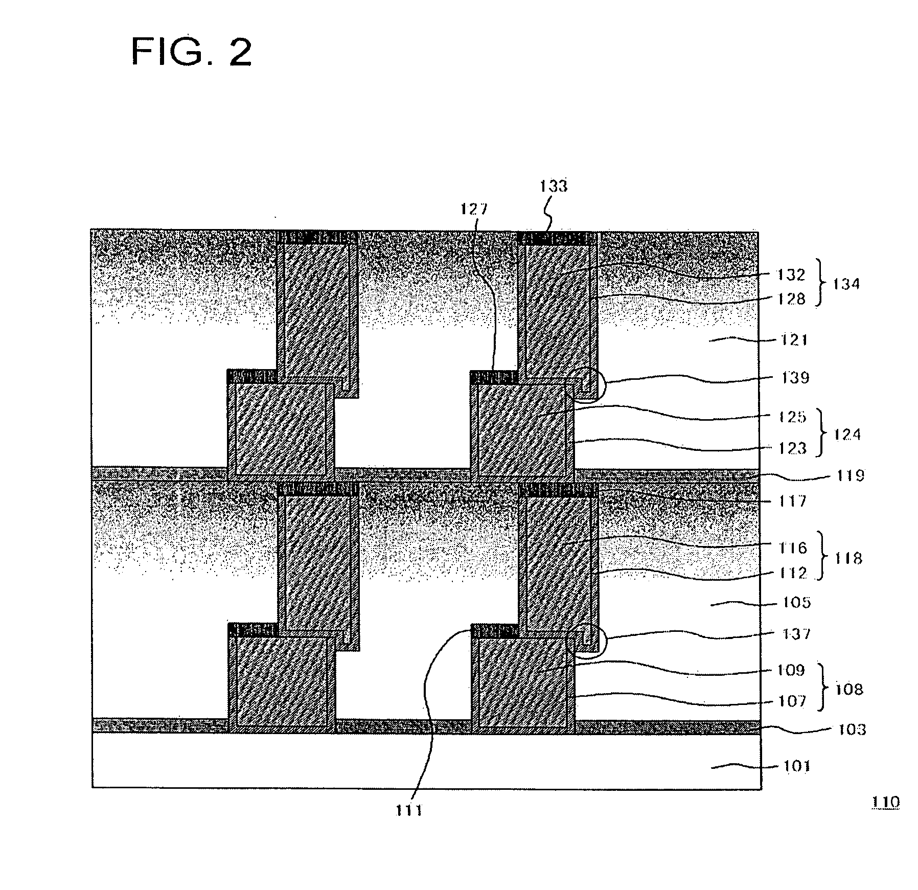
[0047]FIGS. 1 and 2 are cross-sectional views illustrating the configuration of a semiconductor device according to this embodiment. A semiconductor device 110 shown in FIG. 2 is a semiconductor device 100 shown in FIG. 1, in which there is a misalignment in a junction between an interconnect and a via.

[0048] The semiconductor device 100 shown in FIG. 1 has a semiconductor substrate (not shown) and an interconnect structure having a first interconnect 108 made of a copper-containing metal over the semiconductor substrate; a conductive plug (first plug 114) over the first interconnect 108, which is connected to the first interconnect 108; a first cap metal film (Cu silicide layer 111) over the first interconnect 108 in an area other than the area where the first plug 114 is formed; a plug protecting film (Cu silicide layer 117) over the first plug 114; and an insulating film (a first porous MSQ film 105) formed in the region from the side surface of the first interconnect 108 to the...

embodiment 2

[0133] Although there has been described the configuration where the first porous MSQ film 105 and the second porous MSQ film 121 are solid in Embodiment 1, there may be an air gap in an insulating film formed from the sidewall of the first interconnect 108 to the sidewall of the first plug 114 such that it covers the sidewall of the first interconnect 108, the upper portion of the first interconnect 108 and the sidewall of the first plug 114. Furthermore, there may be also an air gap in an insulating film formed from the sidewall of the second interconnect 124 to the sidewall of the second plug 130. This embodiment will describe such an aspect.

[0134]FIGS. 12 and 13 are cross-sectional views illustrating the configuration of the semiconductor device according to this embodiment. The semiconductor device 152 shown in FIG. 13 has the configuration as in the semiconductor device 150 shown in FIG. 12, except that there is generated a misalignment in the junction between an interconnect...

embodiment 3

[0147] The semiconductor device in Embodiment 2 may have a configuration without the first SiC film 103 or the second SiC film 119.

[0148]FIGS. 16 and 17 are cross-sectional views illustrating the configuration of the semiconductor device according to this embodiment. A semiconductor device 162 shown in FIG. 17 has the configuration as in a semiconductor device 160 shown in FIG. 16, except that a misalignment is generated in the junction between an interconnect and a via.

[0149] The semiconductor devices shown in FIGS. 16 and 17 have the basic configurations as described for the semiconductor device 150 (FIG. 12) and the semiconductor device 152 (FIG. 13) in Embodiment 2, respectively, except that the first SiC film 103 or the second SiC film 119 is not formed.

[0150] The semiconductor device 160 and the semiconductor device 162 can be manufactured as described for manufacturing the semiconductor device 150 and the semiconductor device 152 in Embodiment 2,although, after removing th...


PUM


Abstract

An object of this invention is to effectively reduce a connection resistance between a plug and an interconnect, and a dielectric constant of an insulating film.
A semiconductor device 100 has a semiconductor substrate (not shown); a first interconnect 108 made of a copper-containing metal which is formed over the semiconductor substrate; a conductive first plug 114 formed over the first interconnect 108 and connected to the first interconnect 108; a Cu silicide layer 111 over the first interconnect 108 in an area other than the area where the first plug 114 is formed; a Cu silicide layer 117 over the first plug 114; and a first porous MSQ film 105 formed over an area from the side surface of the first interconnect 108 to the side surface of the first plug 114 and covering the side surface of the first interconnect 108, the upper portion of the first interconnect 108 and the side surface of the first plug 114.

Description

[0001] This application is based on Japanese patent application NO. 2005-077720, the content of which is incorporated hereinto by reference. BACKGROUND [0002] 1. Technical Field [0003] This invention relates to a semiconductor device having a multilayer interconnect structure and a manufacturing process therefor. [0004] 2. Related Art FIG. 21 is a cross-sectional view illustrating the configuration of a conventional semiconductor device. The semiconductor device 200 shown in FIG. 21 will be manufactured in accordance with the following procedure. [0005] First, on a silicon substrate (not shown) are formed an SiO2 film 201 and a SiC barrier dielectric film 203. On the barrier dielectric film 203 is then deposited a porous SiOC film as a first Low-k (low dielectric constant) film 205 to a thickness of about 70 to 200 nm. On the first Low-k film 205 is deposited a hard mask SiO2 film (not shown) to a thickness of about 50 to 150 nm. Then, the hard mask SiO2 film and the porous SiOC fil...

Claims


Application Information

Patent Timeline
Patent Type & Authority Applications(United States)
IPC IPC(8): H01L21/4763
CPCH01L21/7682H01L21/76825H01L21/76829H01L21/76852H01L21/76885H01L21/76889H01L23/5222H01L23/53238H01L23/5329H01L23/53295H01L2924/3011H01L2924/0002H01L2924/00
Inventor USAMI, TATSUYA
Owner RENESAS ELECTRONICS CORP
Why Eureka
Try Eureka