Silicon oxide cap over high dielectric constant films

a silicon oxide and dielectric constant technology, applied in the field of silicon oxide cap layer over high dielectric constant material, can solve the problems of low dielectric constant, high defect densities of ultra thin gate oxides (for example, less than 5 nm), pinholes, and charge trapping states, and achieve high defect densities and low dielectric constant. , the effect of reducing the resistance of the gate dielectri

Inactive Publication Date: 2006-09-21
ASM AMERICA INC
View PDF4 Cites 352 Cited by
  • Summary
  • Abstract
  • Description
  • Claims
  • Application Information

AI Technical Summary

Benefits of technology

[0011] In another aspect of the present invention, a semiconductor apparatus comprises an oxide capping layer positioned between a high k gate dielectric material and a gate electrode.

Problems solved by technology

However, ultra thin gate oxides (for example, less than 5 nm) have been found to exhibit high defect densities, including pinholes, charge trapping states, and susceptibility to hot carrier injection effects.
Such high defect densities lead to leakage currents through the gate dielectric.
This results in rapid device breakdown for circuit designs with less than 0.25 μm gate spacing (“sub-quarter-micron technology”).
While care under laboratory conditions can be used to control defect densities, such control has been difficult to achieve under commercial volume fabrication conditions.
Moreover, even if the integrity of the oxide is perfectly maintained, quantum mechanical effects set fundamental limits on the scaling of the gate oxide.
Silicon nitride (Si3N4) has a slightly higher dielectric constant than SiO2 and also demonstrates good diffusion barrier properties, resisting boron penetration, but has demonstrated poor interface properties.

Method used


Image

  • Silicon oxide cap over high dielectric constant films
  • Silicon oxide cap over high dielectric constant films
  • Silicon oxide cap over high dielectric constant films

Examples


Embodiment Construction

Introduction.

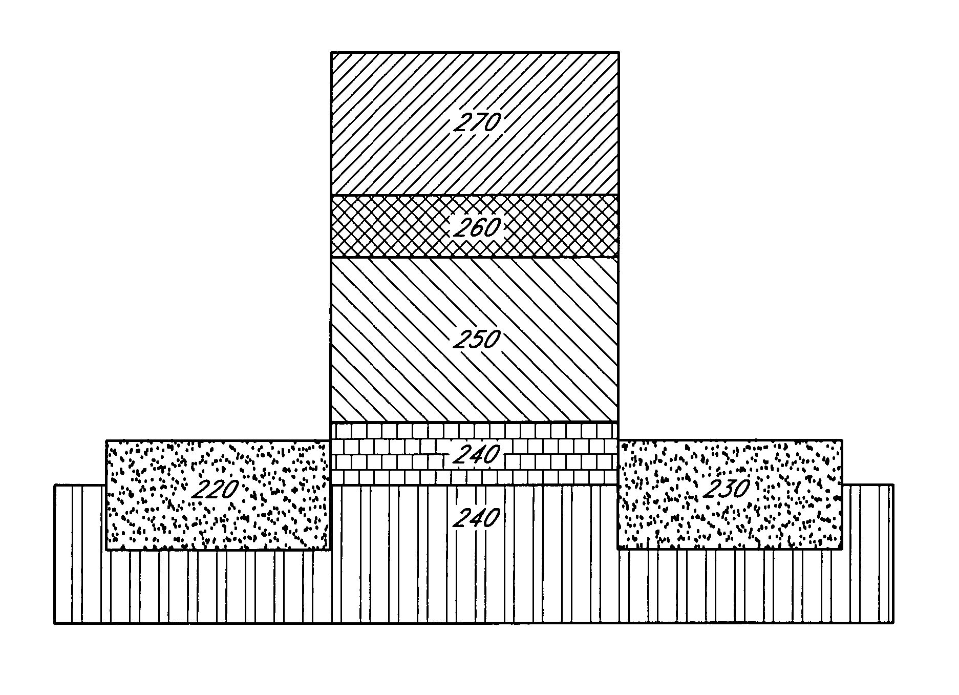
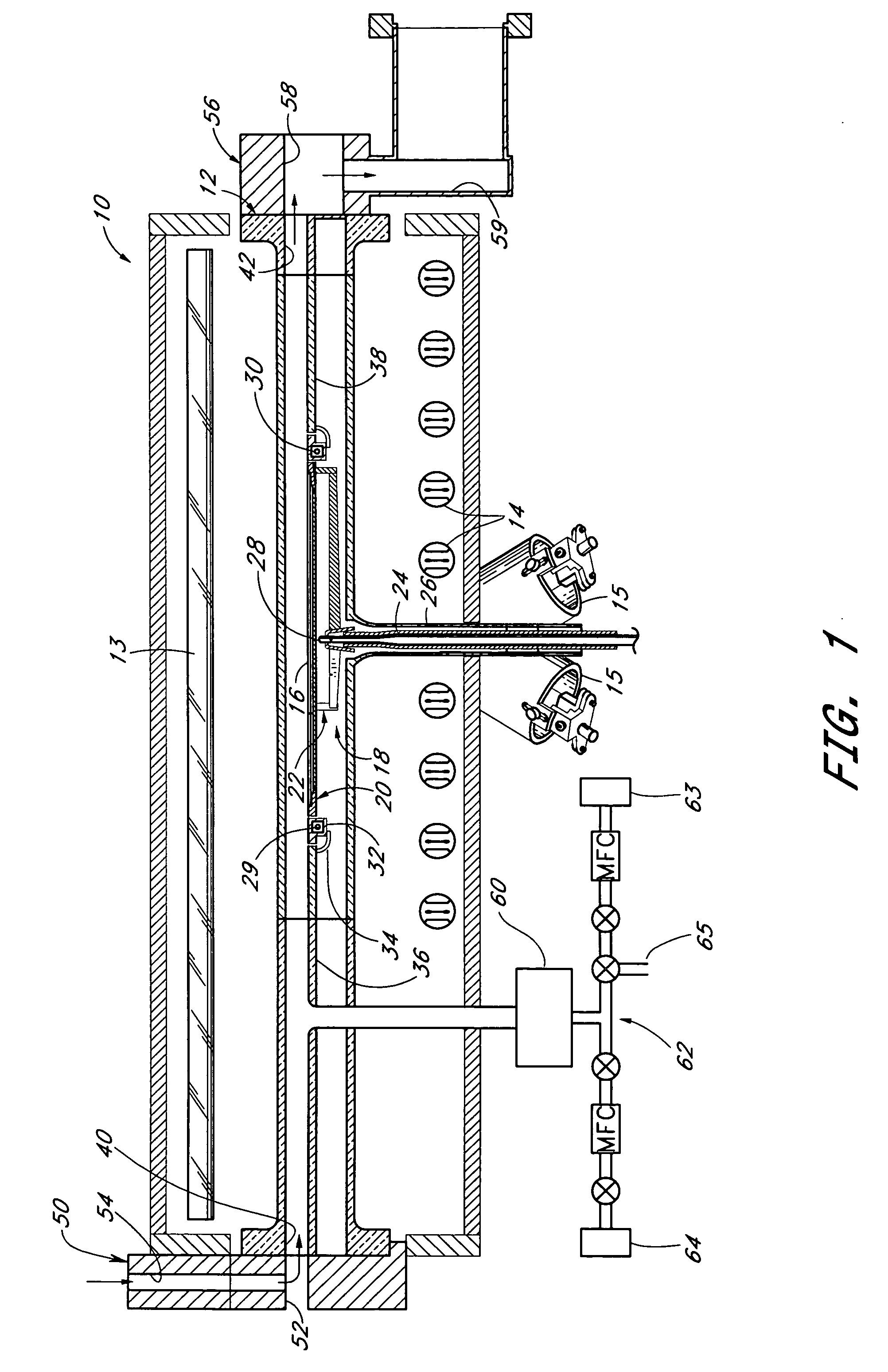
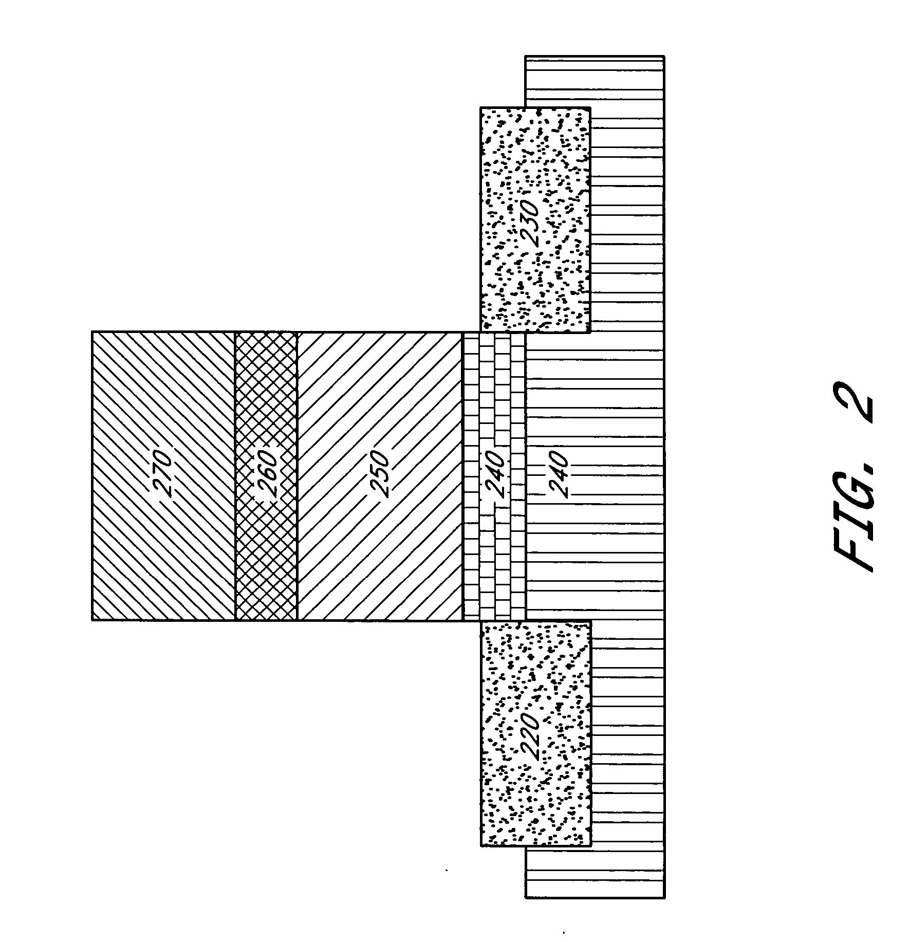
[0022] As described above, high k materials advantageously allow effective electrical gate dielectric thickness to be reduced without introducing deleterious quantum effects. High k layers can be deposited by atomic layer deposition (ALD), which is a chemically self-limiting process, whereby alternated pulses of reaction precursors saturate a substrate and leave no more than one monolayer of material per pulse. Temperatures are maintained above condensation levels and below thermal decomposition levels for the reactants. The precursors are selected to ensure self-saturating reactions, because an adsorbed layer in one pulse leaves a surface termination that is non-reactive with the gas phase reactants of the same pulse. A subsequent pulse of different reactants does react with the previous termination to enable continued deposition. Thus, each cycle of alternated pulses leaves no more than about one molecular layer of the desired material. The principles of ALD type pr...


PUM

PropertyMeasurementUnit
temperatureaaaaaaaaaa

Abstract

A method for forming an integrated circuit structure on a semiconductor substrate comprises depositing a high k gate dielectric material over the substrate using an atomic layer deposition process. A silicon oxide capping layer is deposited over the gate dielectric material in a rapid thermal chemical vapor deposition process. A gate electrode is formed over the silicon oxide capping layer.

Description

FIELD OF THE INVENTION [0001] The present invention relates generally to forming semiconductor layers in integrated circuit fabrication, and relates more specifically to formation of a silicon oxide cap layer over a high dielectric constant material. BACKGROUND OF THE INVENTION [0002] The thin film transistor (TFT) is a fundamental integrated circuit component. A TFT is a layered structure that typically includes a gate electrode separated from a semiconductor layer by a thin gate dielectric layer. Although a common acronym for state-of-the-art transistors is MOS, for metal-oxide-silicon, the material of choice for the gate electrode has long been silicon rather than metal. Among other advantages, silicon gate electrodes are able to withstand high temperature processes and enable self-aligned doping processes used for completing the transistor, thus eliminating expensive masking steps. Currently many metal materials are being explored to replace silicon as the gate electrode; this r...

Claims


Application Information

Patent Timeline
Patent Type & Authority Applications(United States)
IPC IPC(8): H01L21/336
CPCC23C16/401C23C16/405C23C16/452C23C16/45504C23C16/45525C23C16/482H01L21/02164H01L21/02181H01L21/02271H01L21/0228H01L21/28194H01L21/3141H01L21/31608H01L21/31645H01L29/4908H01L29/513H01L29/517
Inventor MAES, JAN WILLEMWITTE, HILDE DEPOMAREDE, CHRISTOPHE
Owner ASM AMERICA INC
Why Eureka
Try Eureka