Dummy via for reducing proximity effect and method of using the same

a proximity effect and dummy via technology, applied in the direction of semiconductor devices, semiconductor/solid-state device details, electrical apparatus, etc., can solve the problems of limited optical lithography techniques, and shortened or rounded lines among other distortions, and achieve the limitation of optical lithography techniques

Active Publication Date: 2006-09-28
MICROSOFT TECH LICENSING LLC
View PDF11 Cites 22 Cited by
  • Summary
  • Abstract
  • Description
  • Claims
  • Application Information

AI Technical Summary

Benefits of technology

[0005] Embodiments of the present invention include a dummy via design for an interconnection process, which builds a similar environment for various vias with different pitches to reduce via proximity effects and enlarge process window.

Problems solved by technology

In the semiconductor manufacturing art, the resolutions obtainable using optical lithography techniques is limited by what is known in the art as “proximity effects”, resulting in variations in feature of line width, alterations in pattern shapes, closed contacts or holes, and shortened or rounded lines among other distortions.
Arising from proximity effects, the vias having difference critical dimensions, depending on their different pitches, usually occur and thereby cause defects.
The OPC technique, however, is limited by the size of the added shapes.
For compensating the via proximity effect, the use of OPC technique is difficult to make different-pitch vias obtain an identical via CD.

Method used


Image

  • Dummy via for reducing proximity effect and method of using the same
  • Dummy via for reducing proximity effect and method of using the same
  • Dummy via for reducing proximity effect and method of using the same

Examples


Embodiment Construction

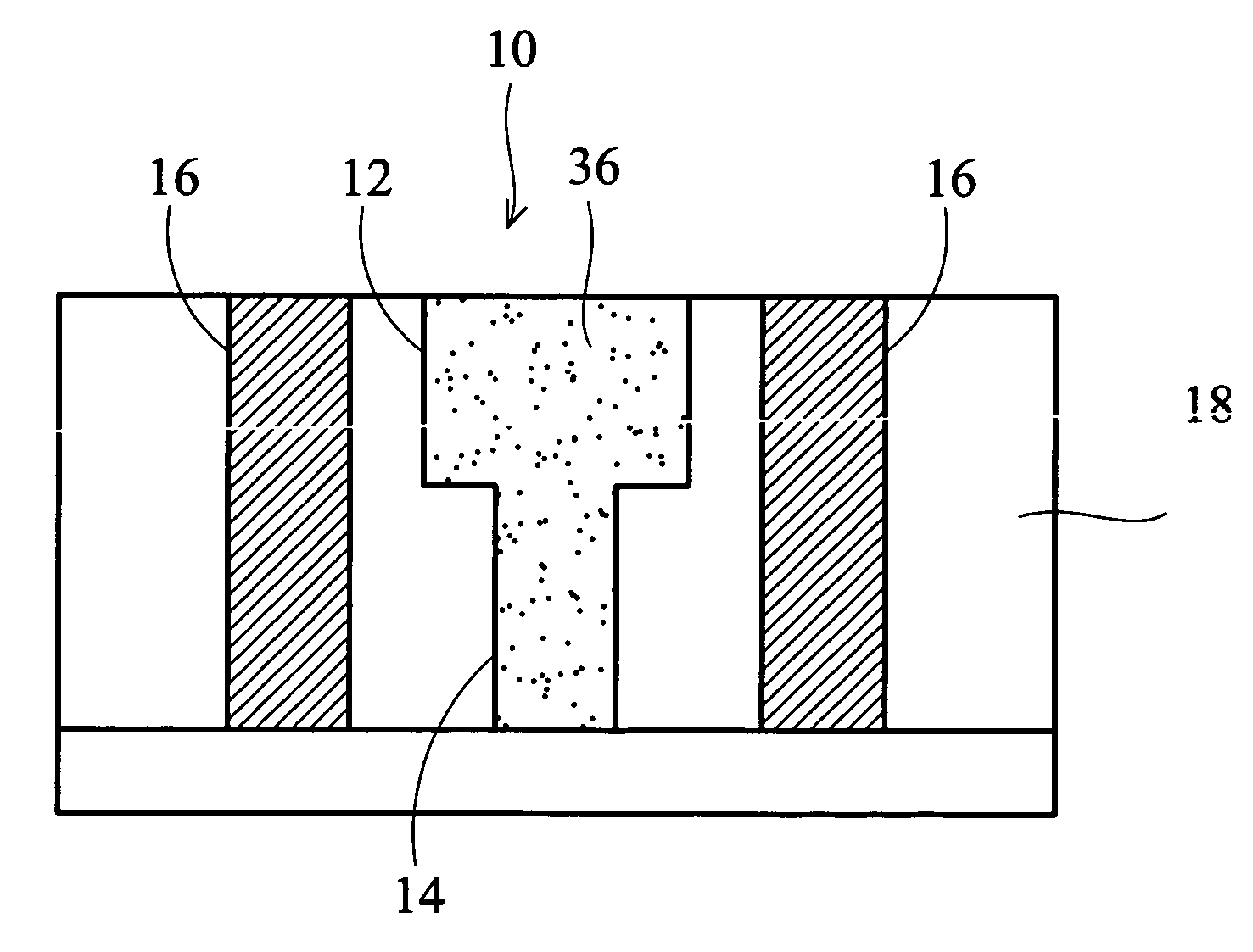
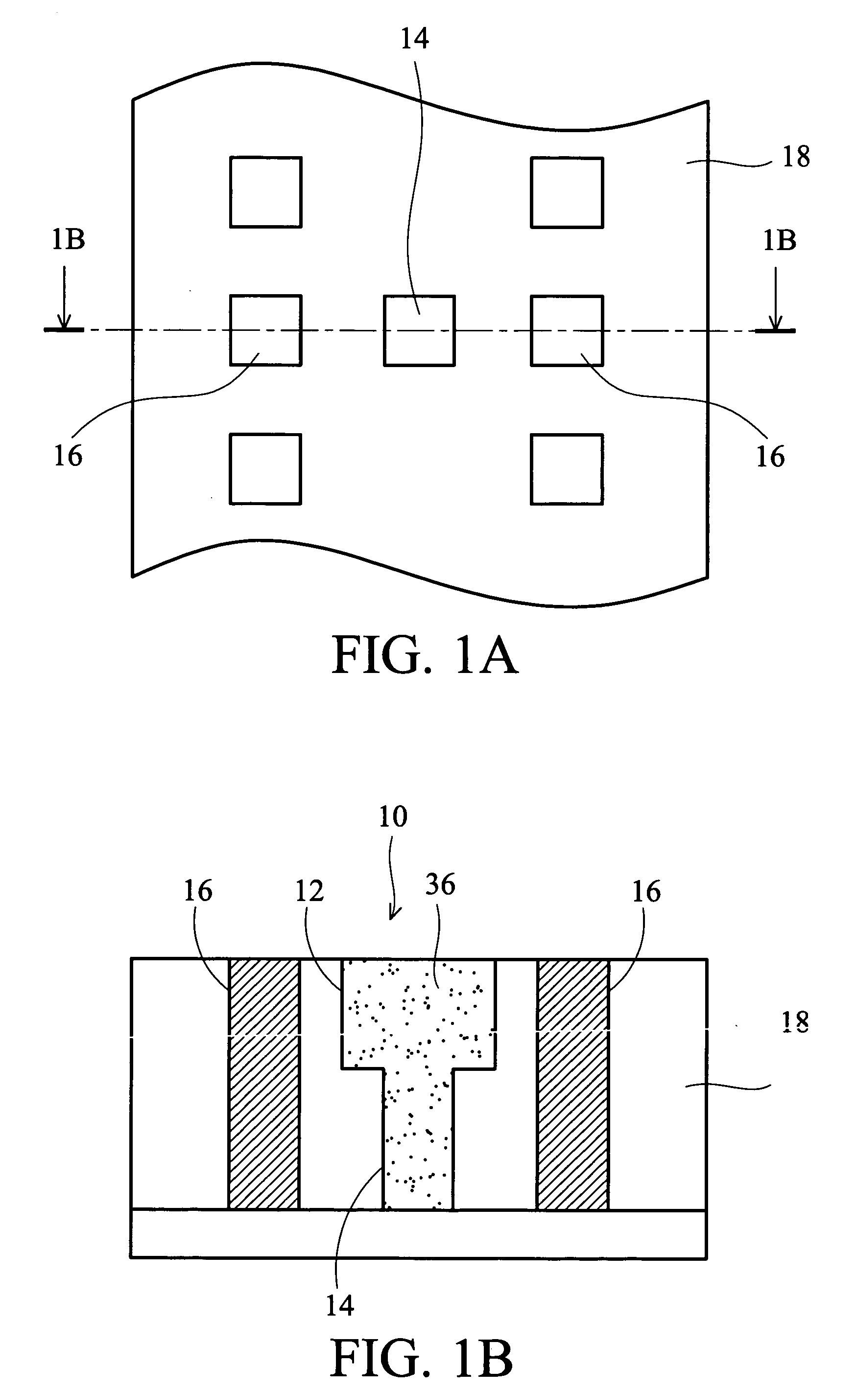
[0012] The present invention provide a dummy via design for an interconnection process, which builds a similar environment for various vias with different pitches to reduce via proximity effects and enlarge process window, thus overcoming the aforementioned problems of the prior art arising from the use of OPC technique. As will be appreciated by persons skilled in the art from discussion herein, one application is used for a dual damascene process, preferably a via-first dual damascene process, and the other application is used for a contact process.

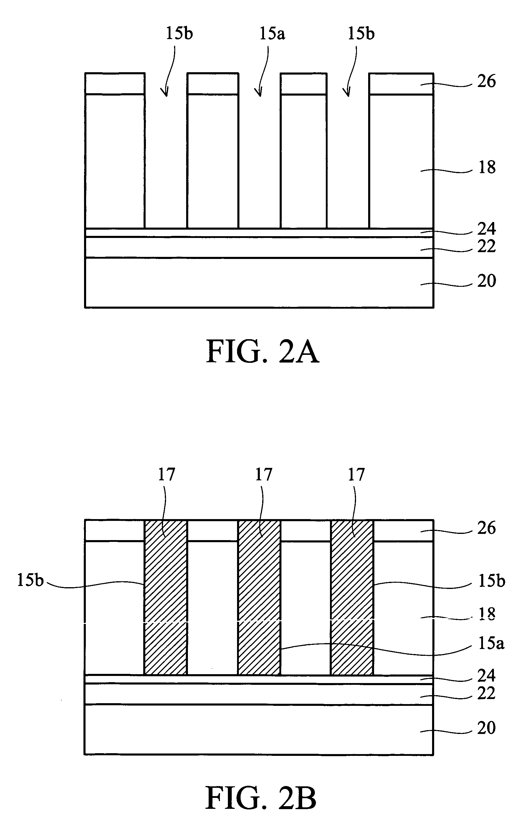
[0013] Reference will now be made in detail to the present embodiments, examples of which are illustrated in the accompanying drawings. Wherever possible, the same reference numbers are used in the drawings and the description to refer to the same or like parts. In the drawings, the shape and thickness of one embodiment may be exaggerated for clarity and convenience. This description will be directed in particular to elements forming p...


PUM


Abstract

A dummy via design for a dual damascene structure has a dielectric layer on a substrate, a dual damascene structure filled with a conductive material and inlaid in the dielectric layer, and a dummy via structure filled with a non-conductive material and inlaid in the dielectric layer. The dummy via structure has at least two dummy vias filled with the non-conductive material and located adjacent to two sides of the dual damascene structure respectively.

Description

TECHNICAL FIELD [0001] The present invention relates to integrated circuit interconnection, and particularly to a dual damascene structure and a via-first dual damascene process of forming the same. BACKGROUND [0002] Microelectronic integrated circuits (ICs) based on patterned semiconductor materials are continuing to evolve towards devices with an extremely high density of circuit elements per unit volume. The use of copper (Cu), with twice the conductivity of aluminum and three times the conductivity of tungsten, has been replaced as the interconnect material in advanced ICs manufacture using either single inlay or dual damascene processes. The conventional method of patterning trenches in a via-first dual damascene process involves filling via openings with an organic bottom anti-reflective coating (BARC), applying a photoresist layer on the via plug and then performing trench lithography. The via-first dual damascene process is considered superior in terms of reliable connection...

Claims


Application Information

Patent Timeline
Patent Type & Authority Applications(United States)
IPC IPC(8): H01L21/4763H01L23/52H01L23/48
CPCH01L21/76808H01L21/76816
Inventor HUANG, KUN-CHENGTSENG, H. C.YOU, JCLIU, K. M.CHEN, T. Y.WANG, C. H.TSAI, TIN-LINHUANG, SSU-CHIA
Owner MICROSOFT TECH LICENSING LLC
Why Eureka
Try Eureka