
Semiconductor device and manufacturing method thereof

a semiconductor and manufacturing method technology, applied in semiconductor devices, measurement devices, instruments, etc., can solve the problems of difficult to improve the operation current of n-type and p-type mos transistors, the control of compressive stresses, and the leakage of pn-junction, so as to improve the operation current and the effect of improving the operation curren

Active Publication Date: 2006-10-05
FUJITSU LTD
View PDF12 Cites 69 Cited by
  • Summary
  • Abstract
  • Description
  • Claims
  • Application Information

AI Technical Summary

Benefits of technology

[0014] An object of the present invention is to provide a semiconductor device that intends to improve both the operation currents of first and second conductivity type elements, and contributes further scale-down of element size, without any change in transistor structure and without adding any extra manufacturing step after formation of an element isolation structure, and to provide a manufacturing method of the semiconductor device.

Problems solved by technology

When the compressive stress increases to exceed the elastic limit of the parent crystal of the semiconductor substrate, dislocation, stacking fault, or the like, is generated and it brings about, for example, PN-junction leak.
Therefore, when such an STI element isolation structure is used for a CMOS transistor in which N-type and P-type MOS transistors are formed on the same semiconductor substrate, it is difficult to improve both the operation currents of the N-type and P-type MOS transistors.
Even in this case, however, because compressive stresses applied from the STI element isolation structure to active regions are isotropic, control of the compressive stresses is insufficient, and it is difficult to cope with a CMOS transistor as described above.
On the other hand, however, it is difficult to positively give an active region a strain of a desired intensity in a desired direction so as to improve the operation current in the active region, and it is not expected to considerably improve characteristics by introducing a strain into an active region.
However, even when such a liner nitride film is provided, there still remains pressure on an STI side wall by the silicon oxide of the STI element isolation structure, and it is difficult to reduce the pressure.

Method used


Image

  • Semiconductor device and manufacturing method thereof
  • Semiconductor device and manufacturing method thereof
  • Semiconductor device and manufacturing method thereof

Examples


first embodiment

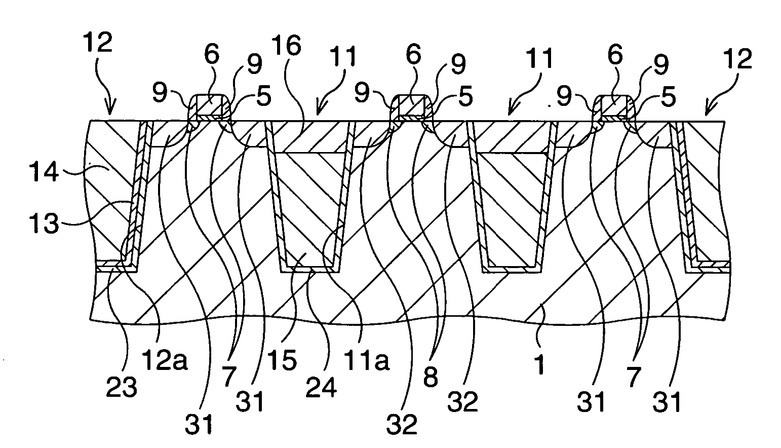
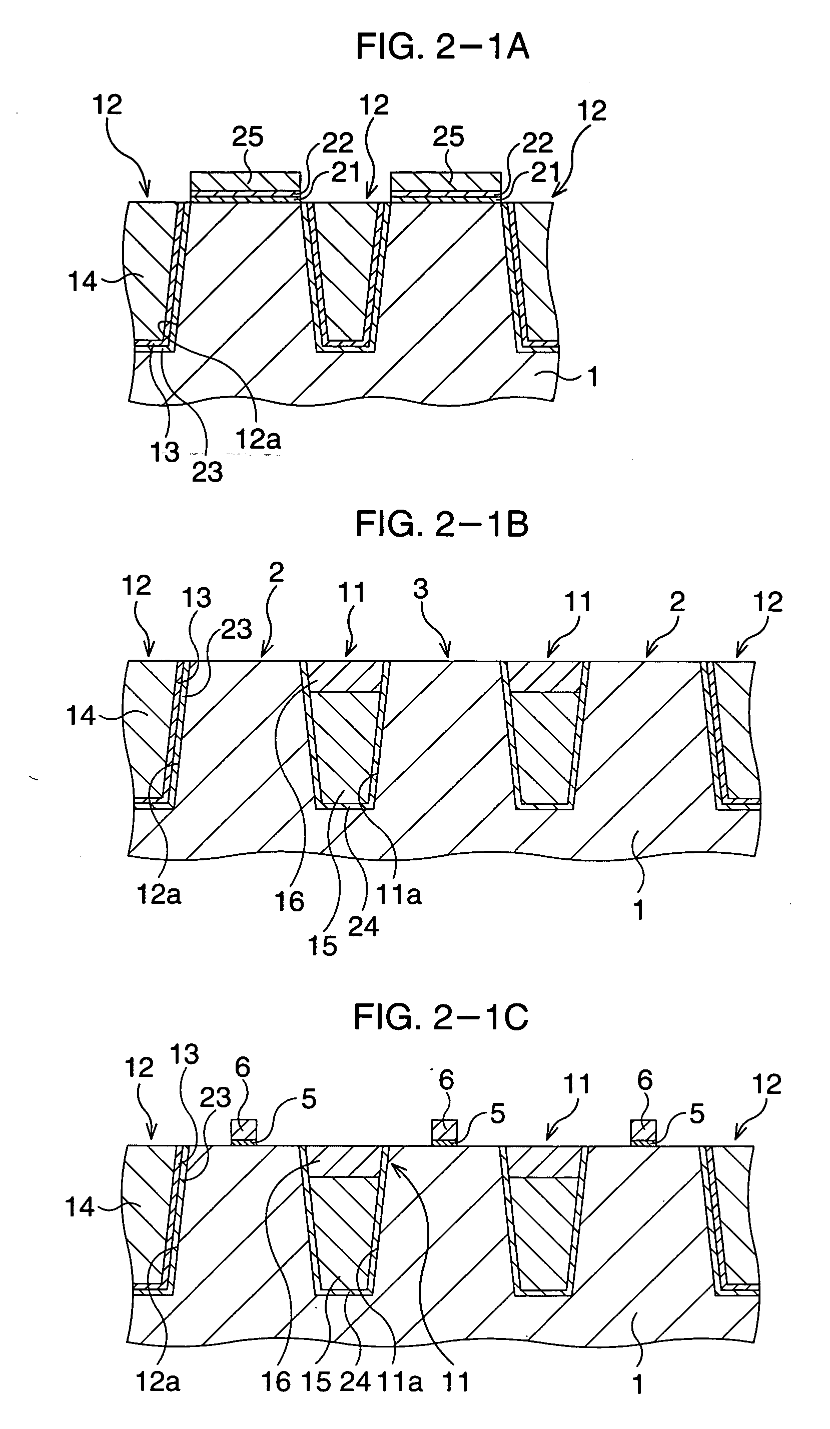
[0050] In this embodiment, a case of a layout in which NMOS transistors and PMOS transistors are alternately arranged will be described, and for convenience's sake of explanation, the construction of a CMOS transistor will be described along its manufacturing process.

[0051]FIGS. 2-1 and 2-2 are schematic sectional views showing a manufacturing method of a CMOS transistor according to this embodiment, in the order of manufacturing steps. FIGS. 3 and 4 are schematic plan views showing particularly principal steps of the manufacturing method of the CMOS transistor according to this embodiment. FIG. 5 is a schematic plan view showing the CMOS transistor completed. FIG. 6 shows schematic sectional views taken along broken lines I-I and II-II in FIG. 4, put in parallel. In FIGS. 2-1 and 2-2, FIG. 2-1A corresponds to the broken line II-II in FIG. 4, and FIGS. 2-1B, 2-1C, and 2-2A to 2-2C correspond to the broken line I-I in FIG. 4.

[0052] In FIGS. 3 to 5, a region where an NMOS transistor...

second embodiment

[0093] A second embodiment of the present invention will be described. In this embodiment will be described a case of a layout in which an NMOS transistor group is constituted by a plurality of NMOS transistors arranged, and each PMOS transistor and the NMOS transistor group are formed in areas on a silicon substrate independent of each other. The same components as in the first embodiment are denoted by the same reference numerals as in the first embodiment.

[0094]FIGS. 10 and 11 are schematic plan views showing particularly principal steps of a manufacturing method of a CMOS transistor according to this embodiment. FIG. 12 shows schematic sectional views taken along broken lines I-I and II-II in FIG. 11, put in parallel.

[0095] In FIGS. 10 and 11, a region where an NMOS transistor is to be formed is represented by NMOS, and a region where a PMOS transistor is to be formed is represented by PMOS. In this embodiment will be described an example in which an NMOS transistor group (thr...

third embodiment

[0126] A third embodiment of the present invention will be described. In this embodiment will be described a case of a layout in which an NMOS transistor group constituted by a plurality of NMOS transistors arranged and a PMOS transistor group constituted by a plurality of PMOS transistors are formed in areas on a silicon substrate independent of each other. The same components as in the first embodiment are denoted by the same reference numerals as in the first embodiment.

[0127]FIGS. 16 and 17 are schematic plan views showing particularly principal steps of a manufacturing method of a CMOS transistor according to this embodiment. FIG. 18 shows schematic sectional views taken along broken lines I-I and II-II in FIG. 17, put in parallel.

[0128] In FIGS. 16 and 17, a region where an NMOS transistor is to be formed is represented by NMOS, and a region where a PMOS transistor is to be formed is represented by PMOS. In this embodiment will be described an example in which an NMOS transi...


PUM


Abstract

The active region of an NMOS transistor and the active region of a PMOS transistor are divided by an STI element isolation structure. The STI element isolation structure is made up of a first element isolation structure formed so as to include the interval between both active regions, and a second element isolation structure formed in the region other than the first element isolation structure.

Description

CROSS-REFERENCE TO RELATED APPLICATIONS [0001] This application is based upon and claims the benefit of priority from the prior Japanese Patent Application No. 2005-104234, filed on Mar. 31, 2005, the entire contents of which are incorporated herein by reference. BACKGROUND OF THE INVENTION [0002] 1. Field of the Invention [0003] The present invention relates to a semiconductor device having an element isolation structure by an STI (Shallow Trench Isolation) method, and also to a manufacturing method of the semiconductor device. [0004] 2. Description of the Related Art [0005] Conventionally, element isolation structures by STI methods, in each of which a trench formed in an element isolation region is filled with an insulating material to ensure electrical insulation between active regions, (hereinafter simply referred to as STI element isolation structures), are used as element isolation structures of semiconductor devices. The STI element isolation structures are expected to meet ...

Claims


Application Information

Patent Timeline
Patent Type & Authority Applications(United States)
IPC IPC(8): H01L29/76
CPCH01L21/76224H01L29/7846H01L21/823878H01L21/823807H01L21/76
Inventor TAMURA, NAOYOSHI
Owner FUJITSU LTD
Features
  • Generate Ideas
  • Intellectual Property
  • Life Sciences
  • Materials
  • Tech Scout
  • Unparalleled Data Quality
  • Higher Quality Content
  • 60% Fewer Hallucinations
Learn More