

Process for producing optical element
a technology of optical elements and polarizing plates, applied in the direction of chemistry apparatus and processes, instruments, transportation and packaging, etc., can solve the problems of inability to provide satisfactory luminance, inability to recycle light, and disadvantageous absorbing of polarizing plates on the lower side, etc., to achieve simple and cost-effective effects
- Summary
- Abstract
- Description
- Claims
- Application Information
AI Technical Summary
Benefits of technology
Problems solved by technology
Method used
Image

Examples
example 1
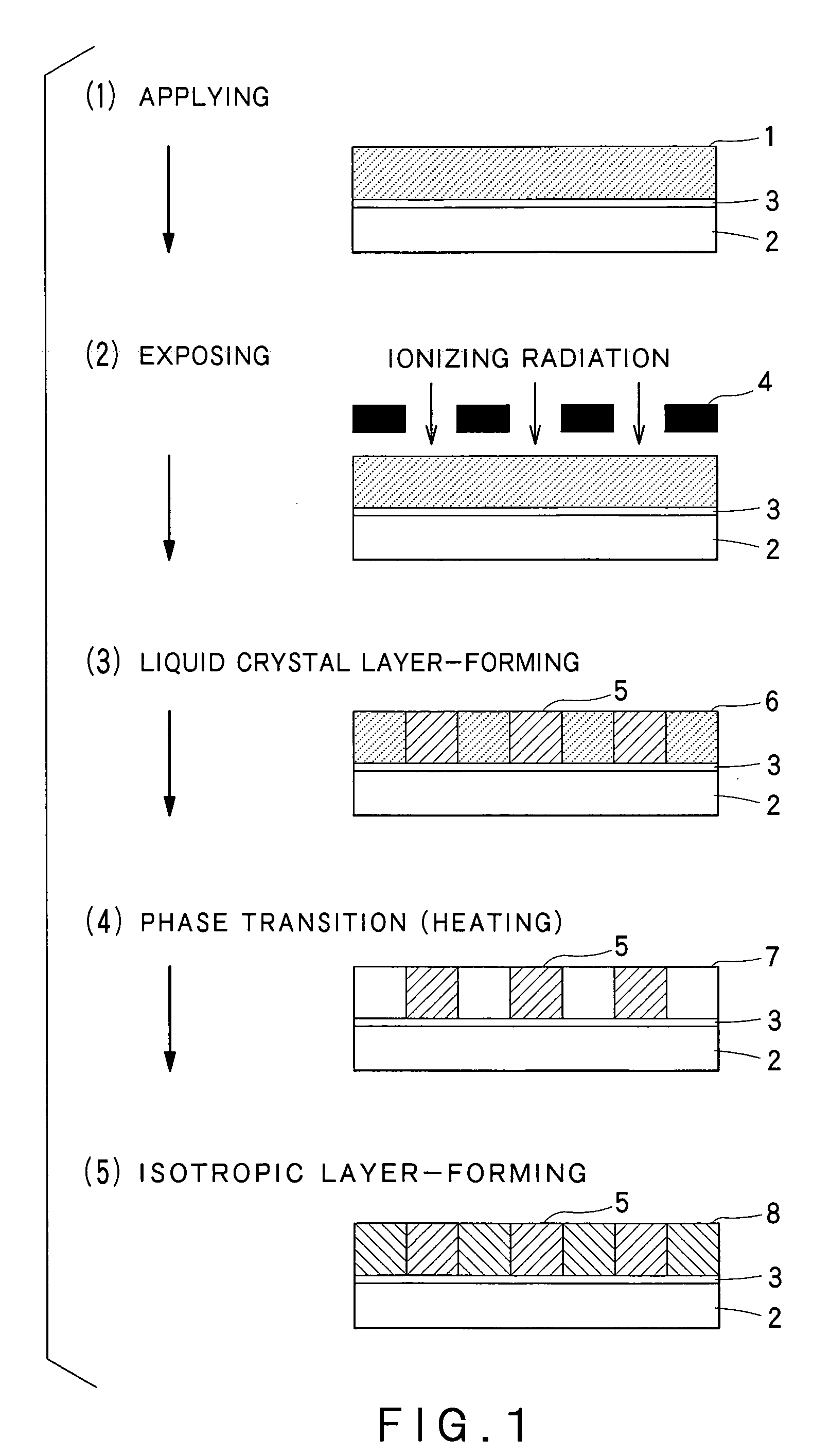
(1) Preparation of Optical Element
[0085] A glass substrate with an aligning film provided thereon was provided as a base material. An aligning film (AL1254) manufactured by JSR, Inc. was spin coated onto a glass base material having a size of 100 mm×100 mm to a coating thickness of 0.065 μm, and the coating was baked at 230° C. in an oven for one hr. The aligning film provided on the base material was then subjected to alignment treatment with a rubbing device.
[0086] Next, a coating liquid having the following composition was spin coated onto the base material to a coating thickness of about 0.8 μm (on a baked state basis).
Polymerizable liquid crystal (RMM 34:23.75 pts.wt.manufactured by Merck & Co. Inc.)Photopolymerization initiator 1.25 pts.wt.(Irg 184: manufactured by Ciba SpecialtyChemicals, K.K.)Solvent (diethylene glycol dimethyl ether) 75 pts.wt.
[0087] Next, the substrate thus formed was held at 80° C. for 3 min to bring the polymerizable liquid crystal to a liquid crys...
example 2
[0091] (1) Preparation of Optical Element
[0092] The same base material as used in Example 1 was used. A coating liquid having the following composition was spin coated onto the base material to a coating thickness of about 0.8 μm (on a baked state basis).
Polymerizable liquid crystal (RMM 34:22.5 pts.wt.manufactured by Merck & Co. Inc.)Photopolymerization initiator1.25 pts.wt.(Irg 184: manufactured by Ciba SpecialtyChemicals, K.K.)Thermal polymerization initiator (AIBN:1.25 pts.wt.manufactured by Wako Pure ChemicalIndustries, Ltd.)Solvent (diethylene glycol dimethyl ether) 75 pts.wt.
[0093] Next, the substrate thus formed was held at 80° C. for 3 min to bring the polymerizable liquid crystal to a liquid crystal phase. When the coating film was changed from an opaque state to a transparent state, it was judged that the phase was transited to a liquid crystal phase. In this state, ultraviolet light was applied onto the coating film through a photomask in any desired form with an ult...
PUM
| Property | Measurement | Unit |
|---|---|---|
| wavelength | aaaaa | aaaaa |
| wavelength | aaaaa | aaaaa |
| thickness | aaaaa | aaaaa |
Abstract
Description
Claims
Application Information