Semiconductor device and method of manufacturing the same

a technology of semiconductor devices and manufacturing methods, which is applied in the direction of printed circuit manufacturing, printed circuit assembling, electrical apparatus construction details, etc., can solve the problems of preventing the attempt to reduce the manufacturing cost of semiconductor devices, and achieve the effect of manufacturing at a lower cos

Active Publication Date: 2006-10-12
RENESAS ELECTRONICS CORP
View PDF21 Cites 51 Cited by
  • Summary
  • Abstract
  • Description
  • Claims
  • Application Information

AI Technical Summary

Benefits of technology

[0006] When forming such semiconductor device, a resin appropriate for fine-scale processing has to be employed on the interconnect layer that faces the semiconductor chip among those constituting the multilayer interconnect structure, for achieving fine-scale connection between the interconnect layer and the semiconductor chip. In contrast, employing the resin appropriate for fine-scale processing is often unnecessary on the interconnect layer that faces the solder balls. As such, it is desirable to employ a relatively inexpensive resin on the interconnect layer facing the solder balls, from the viewpoint of reduction in manufacturing cost of the semiconductor device.
[0007] By the method of manufacturing according to Patent Document 1, however, the interconnect layers are sequentially stacked on the supporting substrate, for constituting the multilayer interconnect structure. Accordingly, the interconnect layer on the side of the solder balls is formed before the formation of the interconnect layer on the side of the semiconductor chip. This imposes a restriction that a resin constituting the interconnect layer on the solder balls side should not have a lower thermal decomposition temperature than a resin constituting the interconnect layer on the semiconductor chip side. Such restriction considerably reduces the selection range of the resin that can be employed for the interconnect layer on the solder balls side, thereby impeding the attempt of lowering the manufacturing cost of the semiconductor device.
[0009] The method of manufacturing thus arranged specifies forming the first interconnect layer, on which the semiconductor chip is to be mounted, on the supporting substrate, while forming the second interconnect layer after the removal of the supporting substrate. Such method removes the restriction against the use of a resin having a lower thermal decomposition temperature than a resin constituting the first interconnect layer, for constituting the second interconnect layer. Therefore, the method allows employing a resin appropriate for fine-scale processing for the first interconnect layer, while employing a relatively inexpensive resin for the second interconnect layer.
[0012] The present invention provides a semiconductor device that can be manufactured at a lower cost, yet allows achieving fine-scale connection between an interconnect layer and a semiconductor chip, and a method of manufacturing such semiconductor device.

Problems solved by technology

In contrast, employing the resin appropriate for fine-scale processing is often unnecessary on the interconnect layer that faces the solder balls.
Such restriction considerably reduces the selection range of the resin that can be employed for the interconnect layer on the solder balls side, thereby impeding the attempt of lowering the manufacturing cost of the semiconductor device.

Method used


Image

  • Semiconductor device and method of manufacturing the same
  • Semiconductor device and method of manufacturing the same
  • Semiconductor device and method of manufacturing the same

Examples


first embodiment

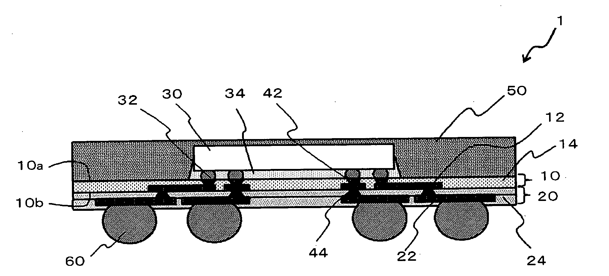
[0029]FIG. 1 is a schematic cross-sectional view showing a semiconductor device according to the first embodiment of the present invention. The semiconductor device 1 includes interconnect layers 10, 20, an IC chip 30, via plugs 42, 44, a seal resin 50, and solder balls 60. In the semiconductor device 1, the IC chip 30, the interconnect layer 10 and the interconnect layer 20 are stacked in this sequence and electrically connected to one another. In other words, the IC chip 30 is mounted on a first surface 10a of the interconnect layer 10, and the interconnect layer 20 is provided on a second surface 10b of the interconnect layer 10, opposite to the first surface 10a.

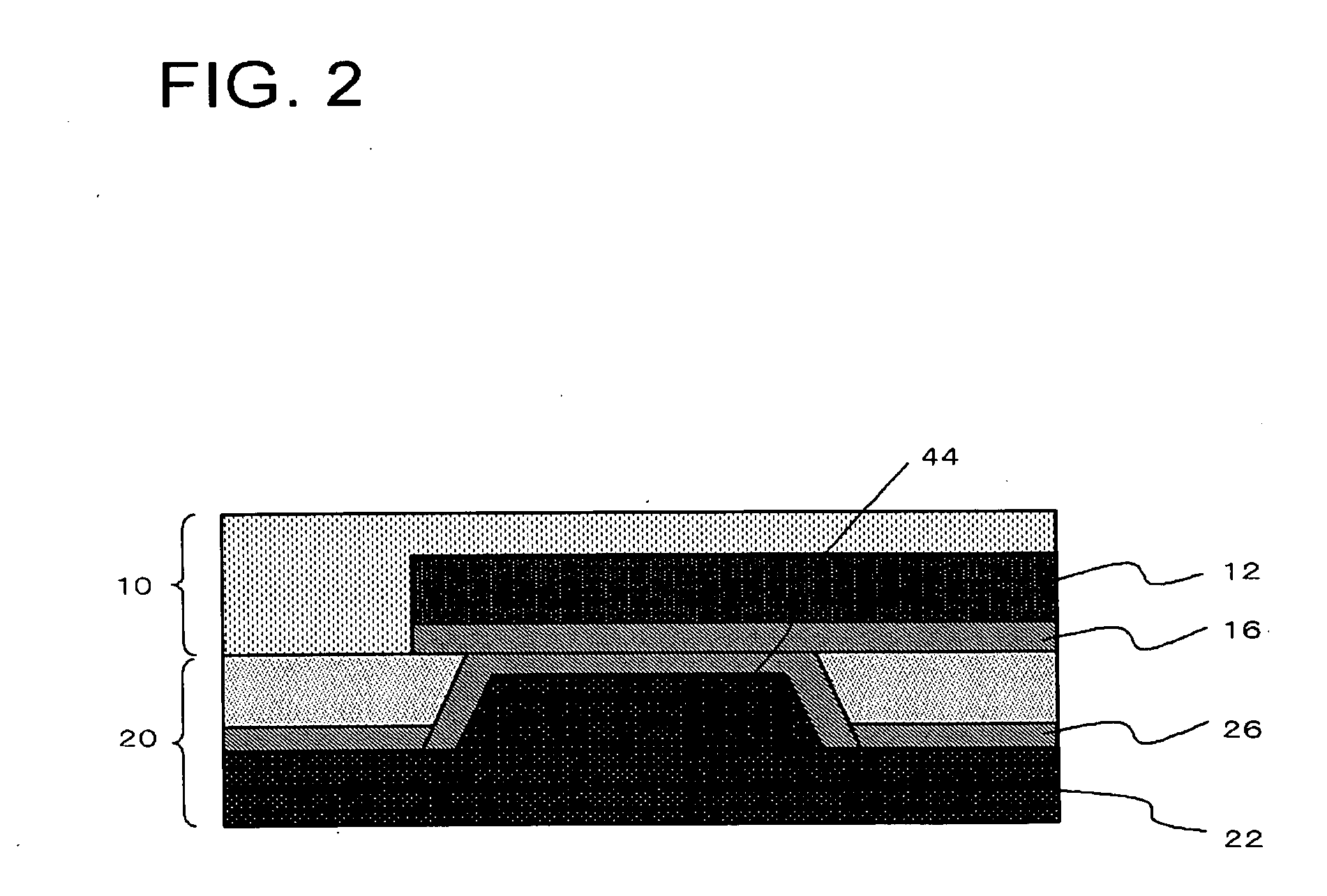
[0030] The interconnect layer 10 (first interconnect layer) includes a conductor interconnect 12 (first interconnect) and an insulating resin 14. The conductor interconnect 12 is buried in a part of the surface layer of the insulating resin 14 facing the interconnect layer 20. Examples of a conductive material employed ...

second embodiment

[0064]FIG. 9 is a schematic cross-sectional view showing a semiconductor device according to the second embodiment of the present invention. The semiconductor device 2 includes interconnect layers 10, 70, an IC chip 30, via plugs 42, 46, a seal resin 50, and solder balls 62, among which the interconnect layer 10, the IC chip 30, the via plug 42 and the seal resin 50 are of the similar structure to those described referring to FIG. 1. In the semiconductor device 2, the IC chip 30, the interconnect layer 10 and the interconnect layer 70 are stacked in this sequence, and electrically connected to one another.

[0065] The interconnect layer 70 (second interconnect layer) includes an insulating resin 74. On the other hand, the interconnect layer 70 is different from the interconnect layer 20 shown in FIG. 1 in not including the conductor interconnect. The insulating resin 74 is constituted of a resin having a lower thermal decomposition temperature than the insulating resin 14.

[0066] The...


PUM

PropertyMeasurementUnit
thermal decomposition temperatureaaaaaaaaaa
conductiveaaaaaaaaaa
areaaaaaaaaaaa

Abstract

The semiconductor device 1 includes interconnect layers 10, 20, an IC chip 30, via plugs 42, 44, a seal resin 50, and solder balls 60. The interconnect layer 10 includes a via plug 42. An end face of the via plug 42 on the side of the interconnect layer 20 is smaller in area than the opposite end face, i.e. the end face on the side of the IC chip 30. An end face of the via plug 44 on the side of the interconnect layer 10 is smaller in area than the opposite end face, i.e. the end face on the side of the solder balls 60. The thermal decomposition temperature of the insulating resin 14 constituting the interconnect layer 10 is higher than that of the insulating resin 24 constituting the interconnect layer 20.

Description

[0001] This application is based on Japanese patent application NO. 2005-109993, the content of which is incorporated hereinto by reference. BACKGROUND [0002] 1. Technical Field [0003] The present invention relates to a semiconductor device and a method of manufacturing the same. [0004] 2. Related Art [0005] Methods of manufacturing a semiconductor device known in the industry include the one disclosed in Japanese Laid-open patent publication NO. 2003-309215 (Patent Document 1). According to the method of manufacturing disclosed therein, a plurality of interconnect layers is sequentially stacked on a supporting substrate thus to form a multilayer interconnect structure, after which the supporting substrate is removed. Then on a surface of the multilayer interconnect structure exposed upon removal of the supporting substrate, solder balls are formed which are to serve as external electrode terminals. On the opposite surface of the multilayer interconnect structure, a semiconductor ch...

Claims


Application Information

Patent Timeline
Patent Type & Authority Applications(United States)
IPC IPC(8): H01L21/00
CPCH01L21/563Y10T29/4913H01L23/3128H01L23/481H01L23/49816H01L23/49822H01L24/81H01L25/0655H01L25/0657H01L2221/68345H01L2221/68359H01L2221/68363H01L2224/16145H01L2224/16225H01L2224/73203H01L2224/73204H01L2224/8121H01L2224/81815H01L2224/83051H01L2225/06513H01L2225/06517H01L2225/06541H01L2225/06572H01L2225/06582H01L2225/06586H01L2924/01078H01L2924/01079H01L2924/15192H01L2924/15311H01L2924/18161H01L2924/19041H05K3/4644H05K3/4676H05K3/4688H01L21/6835H01L2224/16235H01L2224/32225H01L2224/32145H01L2924/00H01L2224/16146H01L2224/17181H01L2224/81005H01L2224/83005H01L2924/00011H01L2924/00014H01L2924/14H01L2224/0401
Inventor KURITA, YOICHIROKAWANO, MASAYASOEJIMA, KOJI
Owner RENESAS ELECTRONICS CORP
Why Eureka
Try Eureka