Semiconductor laser apparatus, method of manufacturing semiconductor laser apparatus, and optical pickup apparatus

a laser apparatus and semiconductor technology, applied in the direction of lasers, semiconductor lasers, solid-state devices, etc., can solve the problems of reducing costs, simplifying configurations, and difficult miniaturizing dvd drives, and significantly difficult to integrate blue-violet semiconductor laser devices, together with infrared semiconductor laser devices and red semiconductor laser devices, into one chip

Inactive Publication Date: 2006-10-12
SANYO ELECTRIC CO LTD
View PDF6 Cites 15 Cited by
  • Summary
  • Abstract
  • Description
  • Claims
  • Application Information

AI Technical Summary

Benefits of technology

[0015] Another object of the present invention is to provide an optical pickup apparatus that can be miniaturized.
[0081] The second semiconductor laser device and the third semiconductor laser device are integrated by the second substrate, so that the second and third emission points are easy to position with respect to the first emission point.

Problems solved by technology

Since the number of components is increased in these methods, however, it is difficult to miniaturize the DVD drives, simplify the configurations, and reduce the costs.
On the other hand, the blue-violet semiconductor laser devices are not formed on GaAs substrates, so that it is significantly difficult to integrate both the blue-violet semiconductor laser devices, together with the infrared semiconductor laser devices and red semiconductor laser devices, into one chips.
Consequently, it is difficult to miniaturize the optical disk recording / reproducing apparatus.

Method used


Image

  • Semiconductor laser apparatus, method of manufacturing semiconductor laser apparatus, and optical pickup apparatus
  • Semiconductor laser apparatus, method of manufacturing semiconductor laser apparatus, and optical pickup apparatus
  • Semiconductor laser apparatus, method of manufacturing semiconductor laser apparatus, and optical pickup apparatus

Examples


first embodiment

(1) First Embodiment

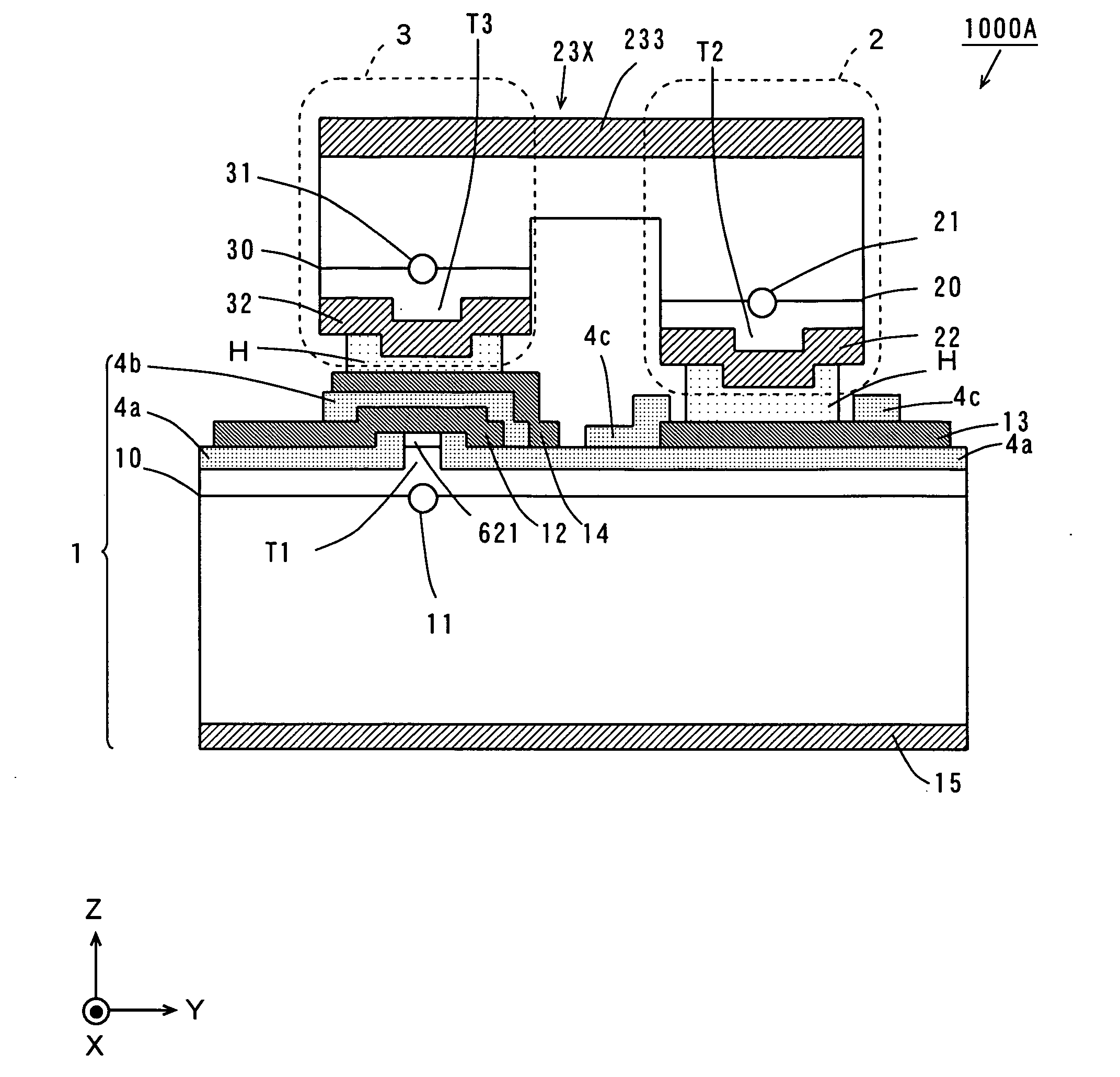
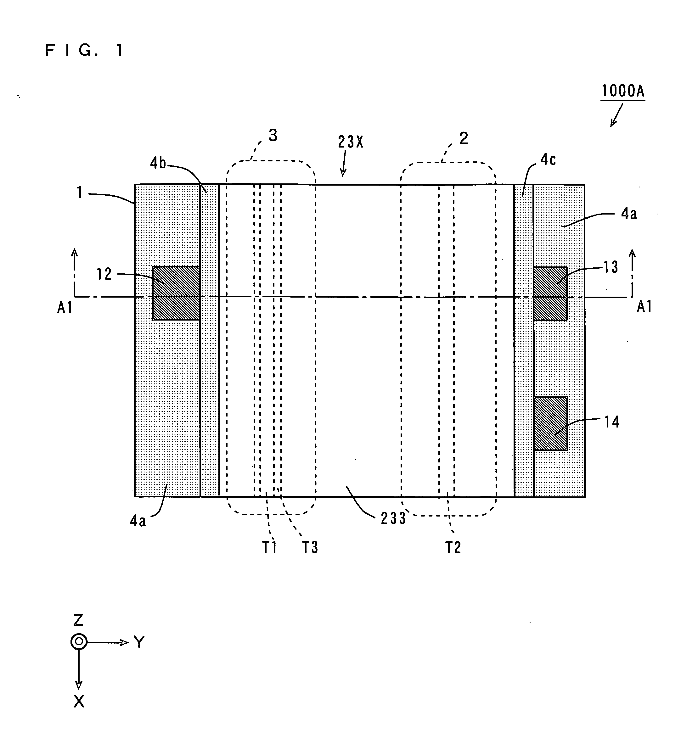
[0124] A semiconductor laser apparatus according to a first embodiment of the present invention comprises a semiconductor laser device emitting a laser beam having a wavelength of approximately 405 nm (hereinafter referred to as a blue-violet semiconductor laser device), a semiconductor laser device emitting a laser beam having a wavelength of approximately 650 nm (hereinafter referred to as a red semiconductor laser device), and a semiconductor laser device emitting a laser beam having a wavelength of approximately 780 nm (hereinafter referred to as an infrared semiconductor laser device).

[0125] (a) Configuration of Semiconductor Laser Apparatus

[0126]FIGS. 1 and 2 are schematic views for explaining the configuration of a semiconductor laser apparatus according to a first embodiment. FIG. 1 is a top view showing an example of the semiconductor laser apparatus according to the first embodiment, and FIG. 2 is a cross-sectional view taken along a line A1-A1 shown ...

second embodiment

(2) Second Embodiment

[0330] A semiconductor laser apparatus according to a second embodiment has the same configuration as the semiconductor laser apparatus 1000A according to the first embodiment except for the following points.

[0331]FIG. 21 is a schematic top view for explaining the configuration of a semiconductor laser apparatus 1000B according to the second embodiment.

[0332] As shown in FIG. 21, the semiconductor laser apparatus 1000B according to the present embodiment comprises a blue-violet semiconductor laser device 1 and a monolithic red / infrared semiconductor laser device 23X.

[0333] The monolithic red / infrared semiconductor laser device 23X comprises a red semiconductor laser device 2 and an infrared semiconductor laser device 3, and is joined to the blue-violet semiconductor laser device 1.

[0334] The length in the X-direction of the monolithic red / infrared semiconductor laser device 23X is larger than the length in the X-direction of the blue-violet semiconductor las...

third embodiment

(3) Third Embodiment

[0338] (a) Configuration and Effect of Semiconductor Laser Apparatus

[0339] A semiconductor laser apparatus 1000C according to a third embodiment has the same configuration as the semiconductor laser apparatus 1000A according to the first embodiment except for the following points.

[0340]FIG. 22 is a top view showing an example of the semiconductor laser apparatus according to the third embodiment. FIGS. 23 and 24 are schematic views of a junction plane of a blue-violet semiconductor laser device 1 and a monolithic red / infrared semiconductor laser device 23X in the semiconductor laser apparatus 1000C shown in FIG. 22. The semiconductor laser apparatus 1000C according to the present embodiment has a blue-violet semiconductor laser device 1 and a monolithic red / infrared semiconductor laser device 23X similar to those shown in and 2. A cross-sectional view taken along a line A2-A2 shown in FIG. 22 is identical to the cross-sectional view taken along the line A1-A1 s...


PUM


Abstract

A monolithic red / infrared semiconductor laser device is joined to a blue-violet semiconductor laser device. The distance between a blue-violet emission point in the blue-violet semiconductor laser device and an infrared emission point in an infrared semiconductor laser device is significantly shorter than the distance between a red emission point in a red semiconductor laser device and the infrared emission point. A blue-violet laser beam, a red laser beam, and an infrared laser beam respectively emitted from the blue-violet emission point, the red emission point, and the infrared emission point are introduced into a photodetector after being incident on an optical disk by an optical system comprising a polarizing beam splitter, a collimator lens, a beam expander, a λ / 4 plate, an objective lens, a cylindrical lens, and an optical axis correction element.

Description

BACKGROUND OF THE INVENTION [0001] 1. Field of the Invention [0002] The present invention relates to a semiconductor laser apparatus capable of emitting a plurality of light beams respectively having different wavelengths, a method of manufacturing the semiconductor laser apparatus, and an optical pickup apparatus. [0003] 2. Description of the Background Art [0004] Conventionally, semiconductor laser devices that emit infrared light beams having wavelengths of approximately 780 nm (infrared semiconductor laser devices) have been used as light sources for compact disk (CD) drives. Further, semiconductor laser devices that emit red light beams having wavelengths of approximately 650 nm as light sources (red semiconductor laser devices) have been used for conventional digital versatile disk (DVD) drives. [0005] On the other hand, DVDs capable of recording and reproduction using blue-violet light beams having wavelengths of approximately 405 nm have been developed in recent years. In or...

Claims


Application Information

Patent Timeline
Patent Type & Authority Applications(United States)
IPC IPC(8): H01S5/00
CPCH01S5/4087H01S5/02212H01S5/4043H01S5/02276H01S5/02272H01L2224/48091H01S5/0237H01S5/02345
Inventor HATA, MASAYUKIBESSHO, YASUYUKINOMURA, YASUHIKOSHONO, MASAYUKINAGATOMI, KENJITSUCHIYA, YOICHI
Owner SANYO ELECTRIC CO LTD
Why Eureka
Try Eureka