

Method for making a semiconductor device with strain enhancement
a technology of strain enhancement and semiconductor devices, applied in the direction of semiconductor devices, basic electric elements, electrical appliances, etc., can solve the problems of reducing the amount of stress the stressor material provides, unable to achieve a transistor with high strain with permissible defectivity control, and increasing the amount of transistor current leakag
- Summary
- Abstract
- Description
- Claims
- Application Information
AI Technical Summary
Problems solved by technology
Method used
Image

Examples
Embodiment Construction
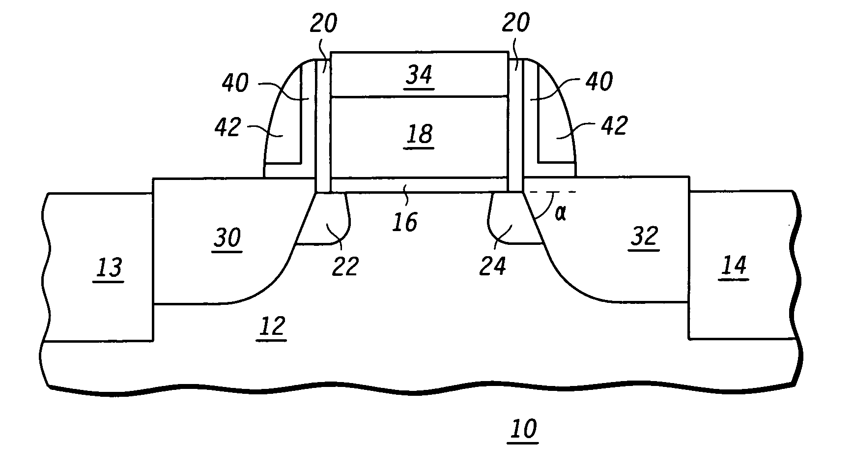
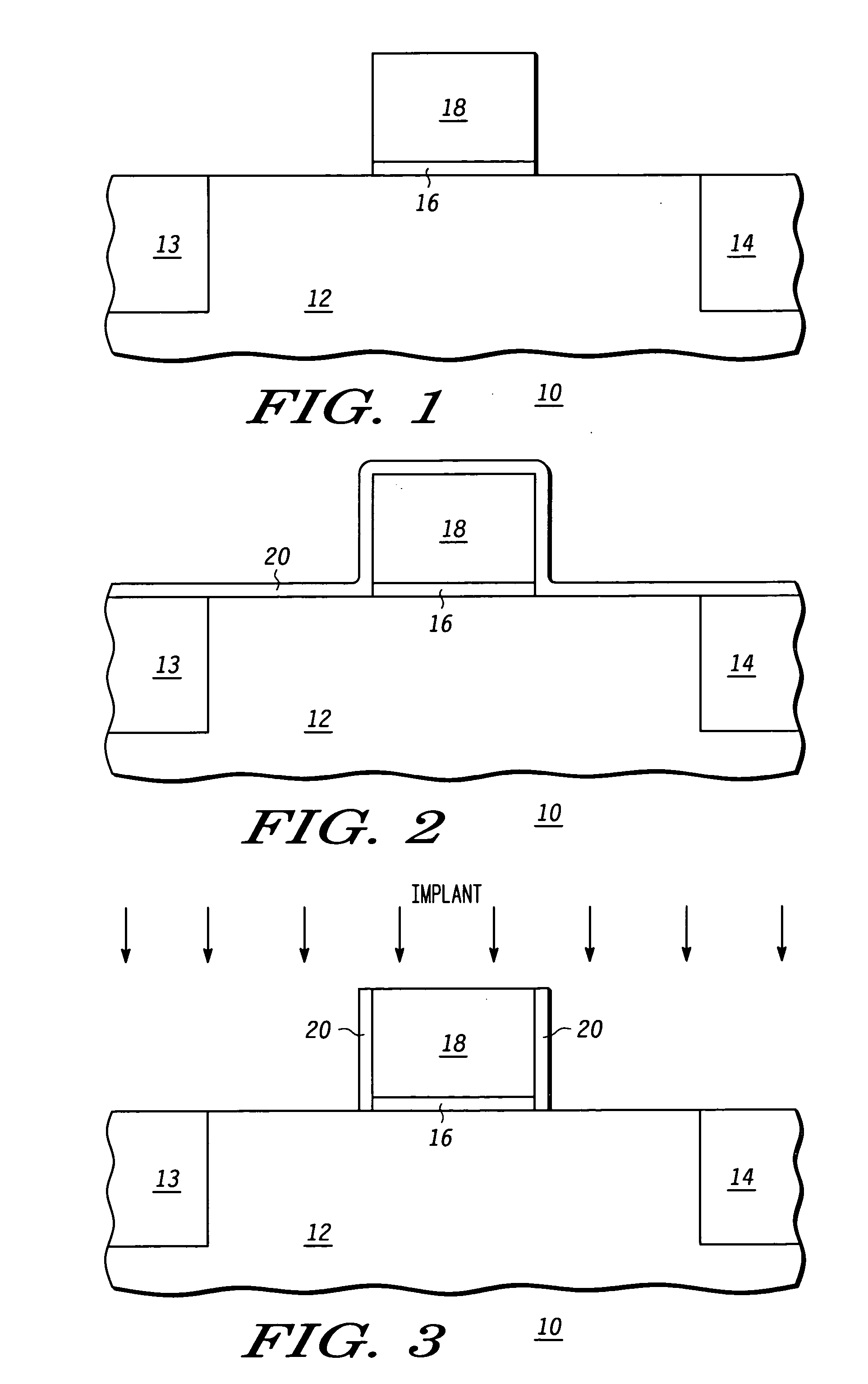
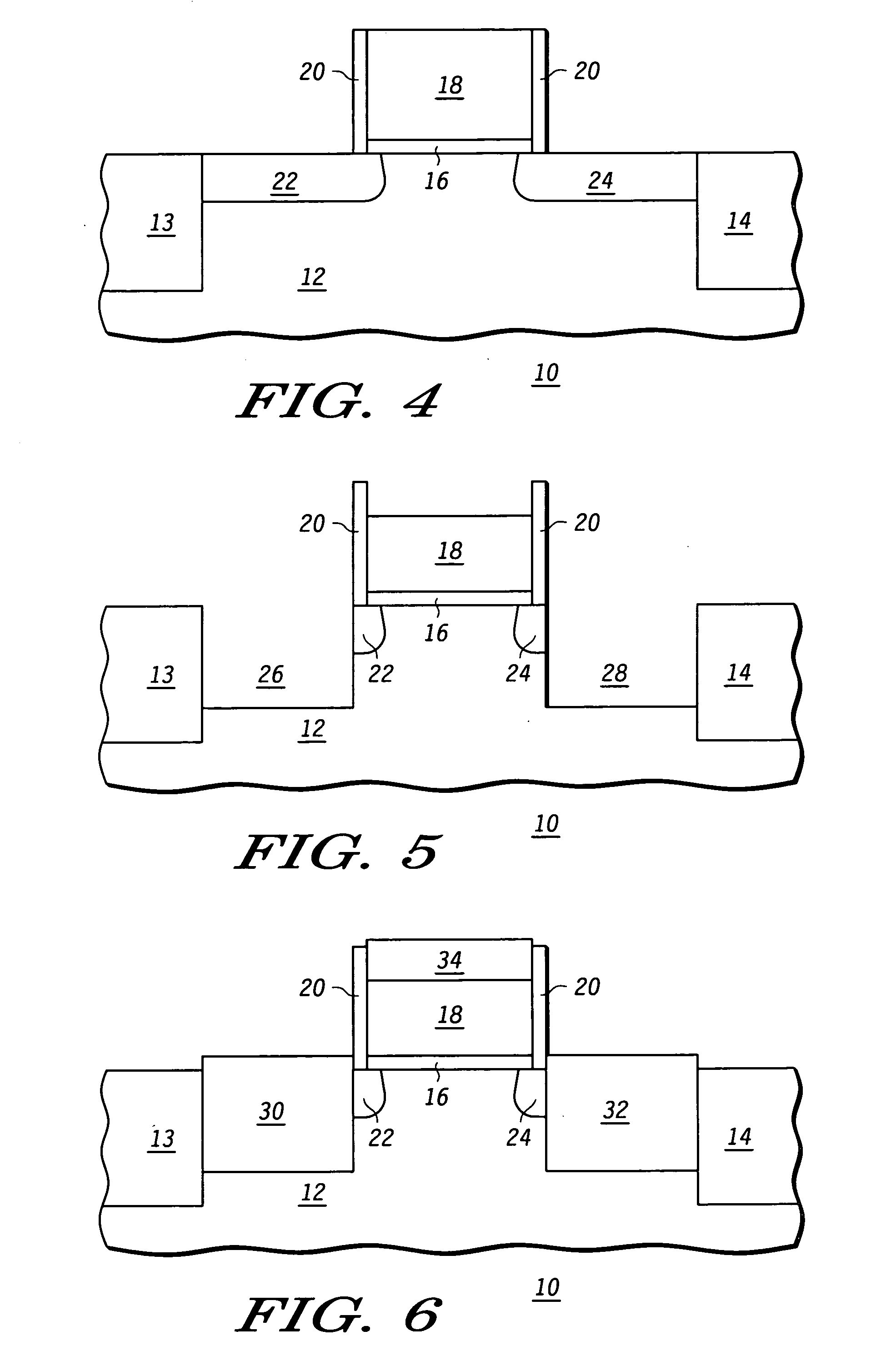
[0012]FIG. 1 illustrates a cross-sectional view of a semiconductor device 10 wherein a semiconductor substrate 12 is provided. The semiconductor substrate 12 may be of various semiconductor materials such as single crystal silicon, gallium arsenide and other materials. Within semiconductor substrate 12 is an isolation trench 13 and an isolation trench 14 for providing electrical isolation within the semiconductor substrate 12. Overlying the semiconductor substrate 12 is an insulating layer 16. In one form the insulating layer 16 is an oxide such as silicon dioxide. Other dielectrics such as silicon oxynitride and high k dielectrics may be used. Overlying the insulating layer 16 is a control electrode or a gate 18. Both the gate 18 and the insulating layer 16 have been patterned in a conventional manner to overlie only a desired portion of the semiconductor substrate 12. The gate 18 is made of a conductive material such as polysilicon or metal, for example. Insulating layer 16 will t...
PUM
 Abstract
Description
Claims
Application Information