Flip chip type nitride semiconductor light emitting device

a technology of nitride semiconductor and light-emitting device, which is applied in the direction of semiconductor/solid-state device details, glass wings, special doors/window arrangements, etc., can solve the problems of low transmission ratio of transparent electrode at 60% to 70%, current leakage, and difficulty in forming ohmic conta

Active Publication Date: 2006-10-19
SAMSUNG ELECTRONICS CO LTD
View PDF11 Cites 20 Cited by
  • Summary
  • Abstract
  • Description
  • Claims
  • Application Information

AI Technical Summary

Benefits of technology

[0019] In another embodiment of the present invention, the flip chip type nitride semiconductor light emitting device may further include a bumping buffer layer made of...

Problems solved by technology

However, migration tendency of Ag has an effect on GaN dislocation, presenting a problem of possible current leakage.
Al is stable but has difficulty in forming an ohmic contact.
However, the transmission ratio of the transparent elect...

Method used


Image

  • Flip chip type nitride semiconductor light emitting device
  • Flip chip type nitride semiconductor light emitting device
  • Flip chip type nitride semiconductor light emitting device

Examples


Embodiment Construction

[0026] Preferred embodiments of the present invention will now be described in detail with reference to the accompanying drawings.

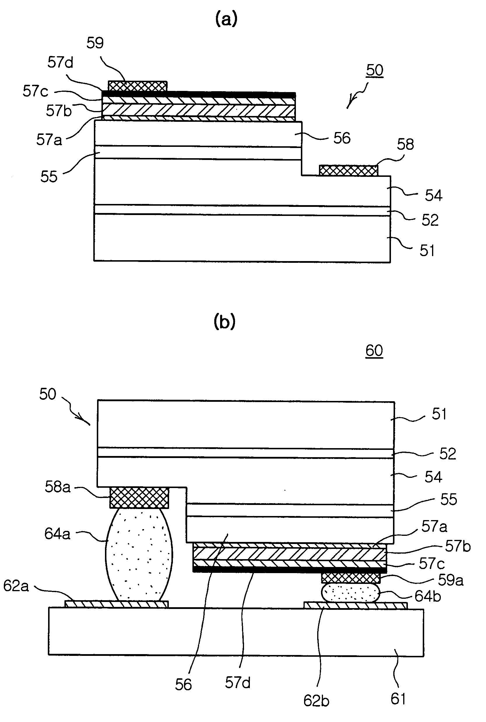
[0027]FIG. 1 is a sectional view illustrating a flip chip type nitride semiconductor light emitting device according to an embodiment of the present invention.

[0028] As shown in FIG. 1, the flip chip type nitride light emitting device 20 includes an n-type nitride semiconductor layer 24, an active area 25, and a p-type nitride semiconductor layer 26 formed in their order on a substrate having a buffer layer 20. The substrate 21 is a light-transmitting substrate which may be a heterogeneous substrate like a sapphire substrate or a homogeneous substrate like a GaN substrate. The exposed upper surface of the n-type nitride semiconductor layer 24 is joined with an n-electrode 28, and the p-type nitride semiconductor layer 26 is joined with a p-electrode 29 through a reflective ohmic contact structure.

[0029] The reflective ohmic contact structure adopted in...


PUM


Abstract

The present invention relates to a flip chip type nitride semiconductor light emitting device having p-type and n-type nitride semiconductor layers, and an active layer in between. The invention also has an ohmic contact layer formed on the p-type nitride semiconductor layer, a light-transmitting conductive oxide layer formed on the ohmic contact layer, and a highly reflective metal layer formed on the light-transmitting conductive oxide layer.

Description

CLAIM OF PRIORITY [0001] This application claims the benefit of Korean Patent Application No. 2005-31682 filed on Apr. 15, 2005, in the Korean Intellectual Property Office, the disclosure of which is incorporated herein by reference. BACKGROUND OF THE INVENTION [0002] 1. Field of the Invention [0003] The present invention relates to a nitride semiconductor light emitting device, and more particularly, to a flip chip type nitride semiconductor light emitting device having a highly reflective ohmic contact structure which can reduce unfavorable effect of reflective metal used while enhancing reflectivity. [0004] 2. Description of the Related Art [0005] In general, a nitride semiconductor constituting a nitride semiconductor light emitting device, more particularly, a p-type nitride semiconductor layer has a wide band gap, having a difficulty in forming an ohmic contact with an electrode. Also, an ohmic contact structure adopted in a flip chip type nitride semiconductor light emitting ...

Claims


Application Information

Patent Timeline
IPC IPC(8): H01L33/00H01L33/32H01L33/10H01L33/42H01L33/62
CPCH01L33/32H01L33/42H01L33/405E06B7/36E06B7/215E06B3/02E05Y2800/41E05Y2800/422
Inventor CHAE, SEUNG WANYOON, SUK KILKO, KUN YOOSHIM, HYUN WOOKYI, BONG IL
Owner SAMSUNG ELECTRONICS CO LTD
Why Eureka
Try Eureka