Hybrid crystal orientation CMOS structure for adaptive well biasing and for power and performance enhancement

a cmos structure and crystal orientation technology, applied in the field of integrated semiconductor devices, can solve the problems of negating the favorable effect of adaptive well biasing, increasing the difficulty of chip power and performance optimization, and insufficient techniqu

Active Publication Date: 2006-10-19
GLOBALFOUNDRIES US INC
View PDF14 Cites 50 Cited by
  • Summary
  • Abstract
  • Description
  • Claims
  • Application Information

AI Technical Summary

Benefits of technology

[0008] The present invention provides a semiconductor structure that includes incoporating field effect transistors (FETs) on a SOI substrate region having a device channel capable of being either partially or fully depleted of charger carriers in combination with FETs within a bulk-Si region having a highly doped well body contact which substantially eliminates floating body effects and provides a means to use adaptive well biasing thereby providing a means to control the threshold voltages of the bulk-Si regions FETs with an applied bias on the well terminal.
[0014] a well region underlying said at least one second device and a contact to said well region, wherein said contact stabilizes floating body effects and provides a means for adjusting threshold voltages in field effect transistors (FETs) located in the bulk-Si region through application of a bias voltage.
[0017] In accordance with the present invention, the second device within the bulk-Si region can be formed by implanting the bulk-Si region with a first type dopant to provide a well region, forming at least one gate region atop a surface of the bulk-Si region, forming source and drain regions adjacent at least one gate region with a second type dopant, and forming a contact to the well region, wherein the contact stabilizes floating body effects and provides a well contact which may be utilized for adjusting the threshold voltages of the devices in the bulk Si region. Forming the contact to the well region comprises etching a portion of the surface of the bulk-Si region to provide a via to the well region and filling the via to the well region with a conductive material.

Problems solved by technology

Optimization of chip power and performance is becoming increasingly challenging as CMOS technologies are scaled to the 90 nm node and beyond.
In SOI CMOS, this technique is not available as the well nodes (bodies) are floating.
The use of body ties structures, however, introduces parasitic resistances and capacitances which would negate the favorable impact of adaptive well biasing.

Method used


Image

  • Hybrid crystal orientation CMOS structure for adaptive well biasing and for power and performance enhancement
  • Hybrid crystal orientation CMOS structure for adaptive well biasing and for power and performance enhancement
  • Hybrid crystal orientation CMOS structure for adaptive well biasing and for power and performance enhancement

Examples


Embodiment Construction

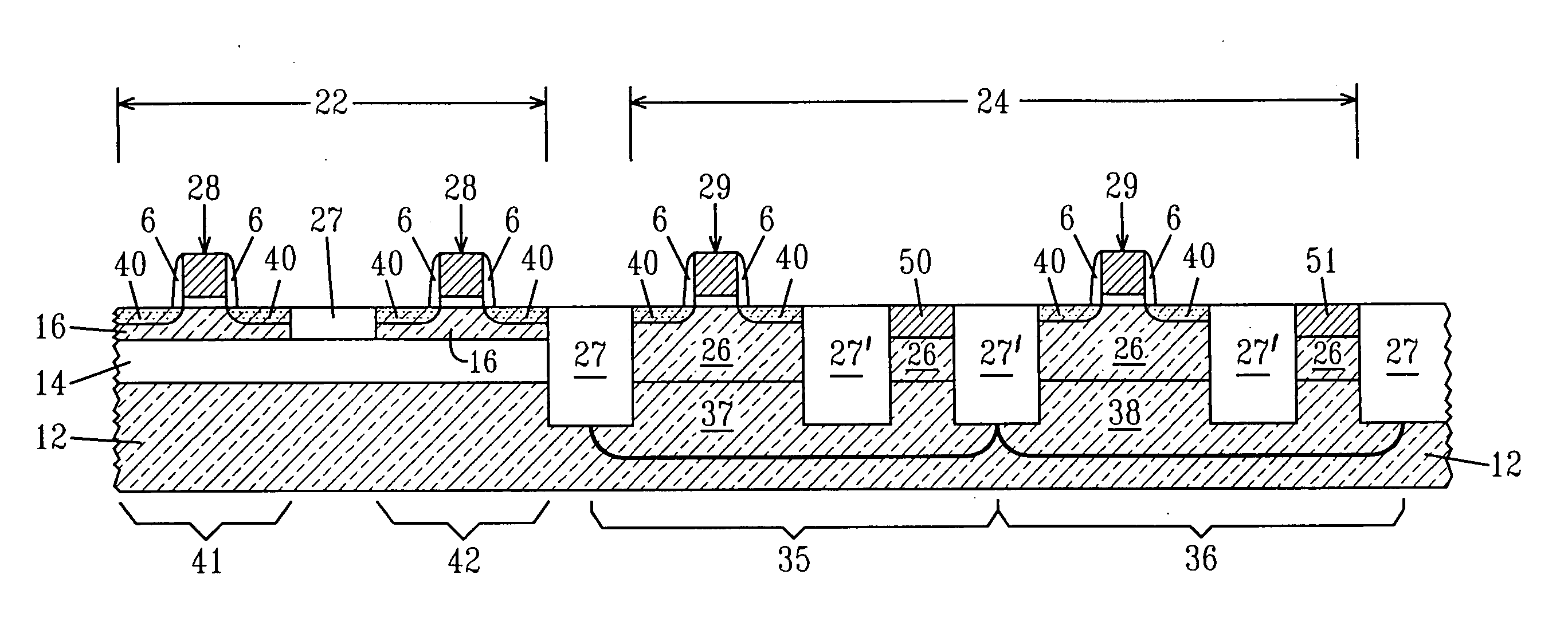
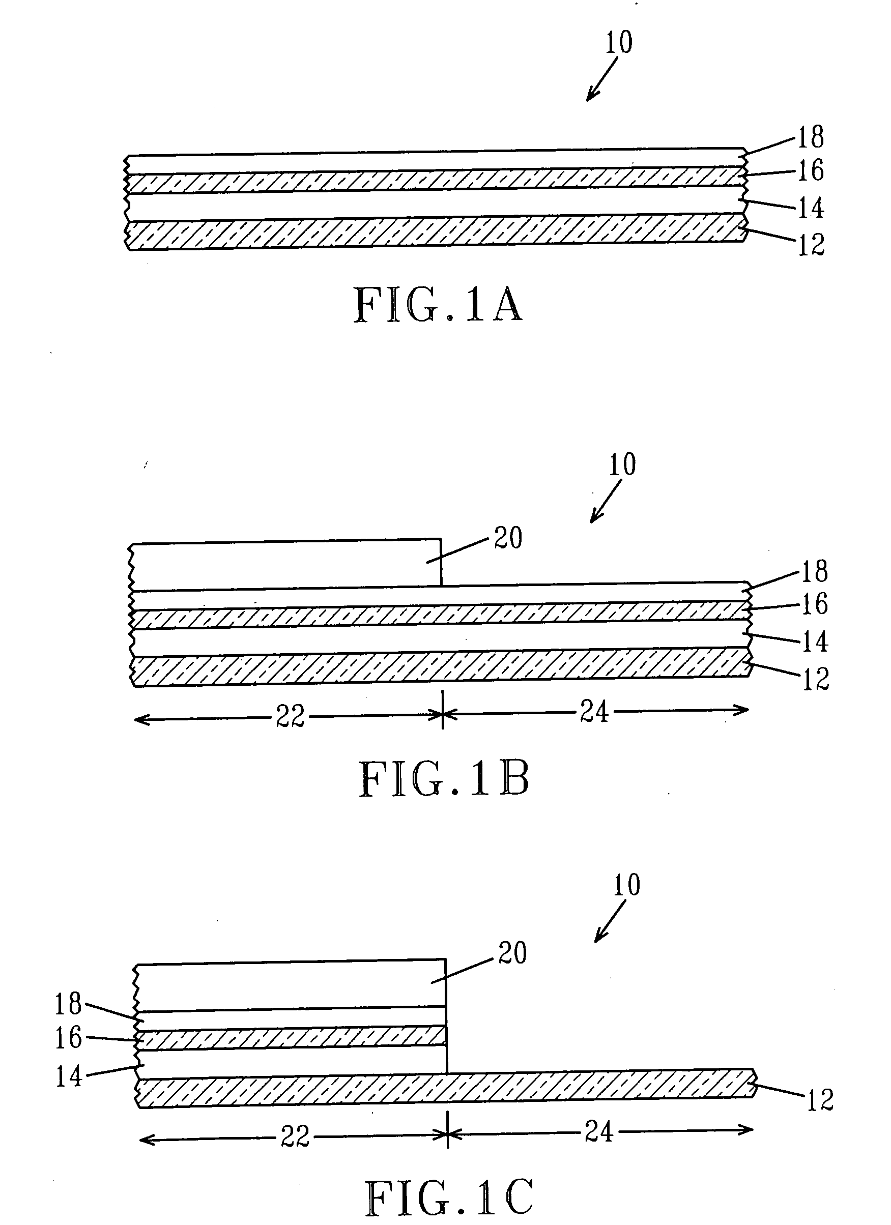
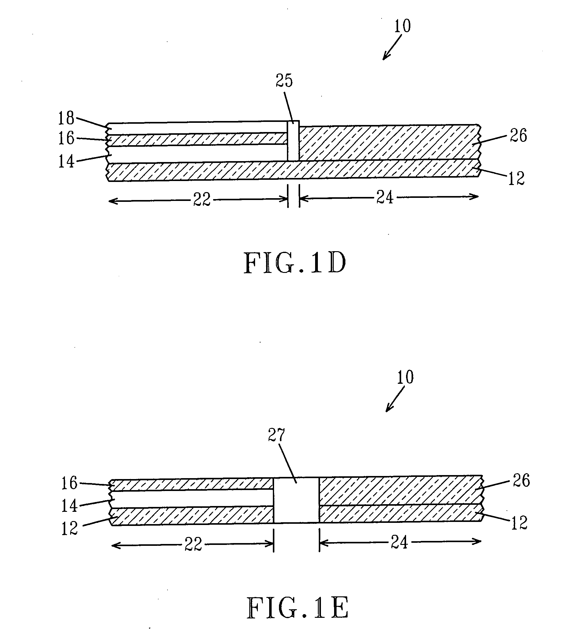
[0020] The present invention, which provides a hybrid crystal orientation CMOS structure for adaptive well biasing and power / performance enhancement, will now be described in greater detail by referring to the following discussion as well as the drawings that accompany the present application. In the accompanying drawings, like and correspondence elements are referred to by like reference numerals. It is noted that the drawings of the present application are provided for illustrative purposes and thus they are not drawn to scale.

[0021]FIG. 1A illustrates a substrate 10, i.e., hybrid substrate, which may be employed in the present invention. As shown, the substrate 10 includes a surface dielectric layer 18, a first semiconductor layer 16, an insulating layer 14, and a second semiconductor layer 12.

[0022] The surface dielectric layer 18 of the substrate 10 is an oxide, nitride, oxynitride or other insulating layer that is either present in one of the initial wafers before bonding, o...


PUM


Abstract

The present invention provides a semiconducting structure including a substrate having an SOI region and a bulk-Si region, wherein the SOI region and the bulk-Si region have a same or differing crystallographic orientation; an isolation region separating the SOI region from the bulk-Si region; and at least one first device located in the SOI region and at least one second device located in the bulk-Si region. The SOI region has an silicon layer atop an insulating layer. The bulk-Si region further comprises a well region underlying the second device and a contact to the well region, wherein the contact stabilizes floating body effects. The well contact is also used to control the threshold voltages of the FETs in the bulk-Si region to optimized the power and performance of circuits built from the combination of the SOI and bulk-Si region FETs.

Description

DESCRIPTION [0001] 1. Field of the Invention [0002] The present invention relates to semiconductor devices, and more particularly to integrated semiconductor devices, such as complementary metal oxide semiconductor (CMOS) devices formed atop a substrate having thin silicon-on-insulator (SOI) and bulk-Si portions, wherein the SOI and bulk-Si portions of the substrate have either the same or different crystalline orientation. In particular, the present invention forms nFET and pFET devices on SOI and bulk-Si regions of a semiconducting substrate having either a surface on a (100), (110), or (111) crystal plane. The bulk-Si region of the substrate is processed to provide devices substantially free of floating body effects that are typically present in the devices formed with SOI substrates. Additionally, in the bulk regions a well contact can be utilized to control the threshold voltage (Vt) of the bulk NFET and pFET devices for improved circuit power and performance. [0003] 2. Backgro...

Claims


Application Information

Patent Timeline
Patent Type & Authority Applications(United States)
IPC IPC(8): H01L27/12
CPCH01L21/823807H01L21/823878H01L27/1207H01L27/1203H01L27/0922
Inventor BERNSTEIN, KERRYSLEIGHT, JEFFREY W.YANG, MIN
Owner GLOBALFOUNDRIES US INC
Why Eureka
Try Eureka