Semiconductor integrated circuit device and I/O cell for the same

a technology of integrated circuit and semiconductor chip, which is applied in the field of semiconductor integrated circuit devices and i/o cells for the same, can solve the problems of increasing wasteful space unused, etc., and achieves the reduction of the area required for the given i/o cell, the effect of reducing the pitch of the i/o cell and reducing the area of the semiconductor chip having

Inactive Publication Date: 2006-10-19
SOCIONEXT INC
View PDF7 Cites 14 Cited by
  • Summary
  • Abstract
  • Description
  • Claims
  • Application Information

AI Technical Summary

Benefits of technology

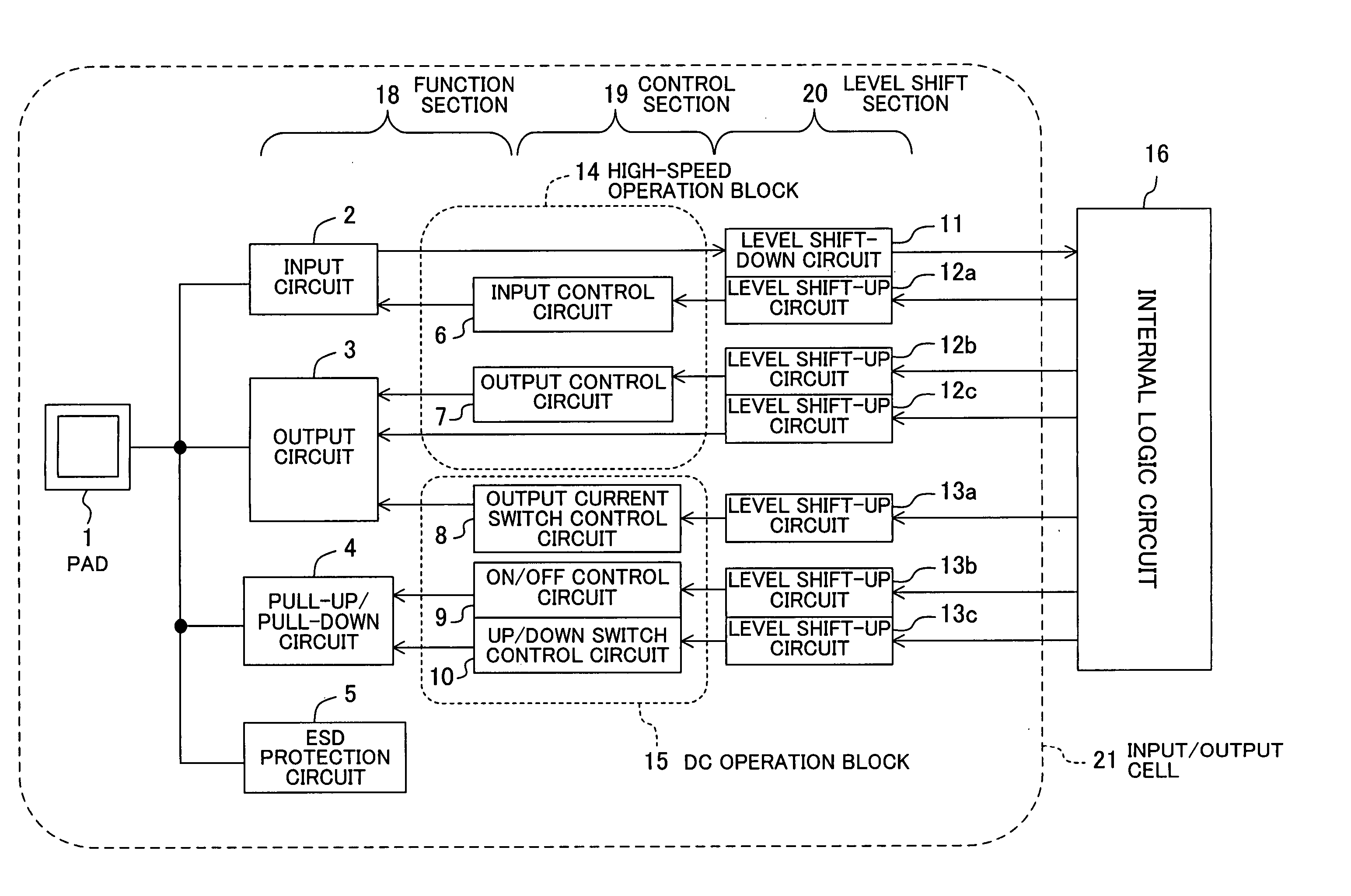
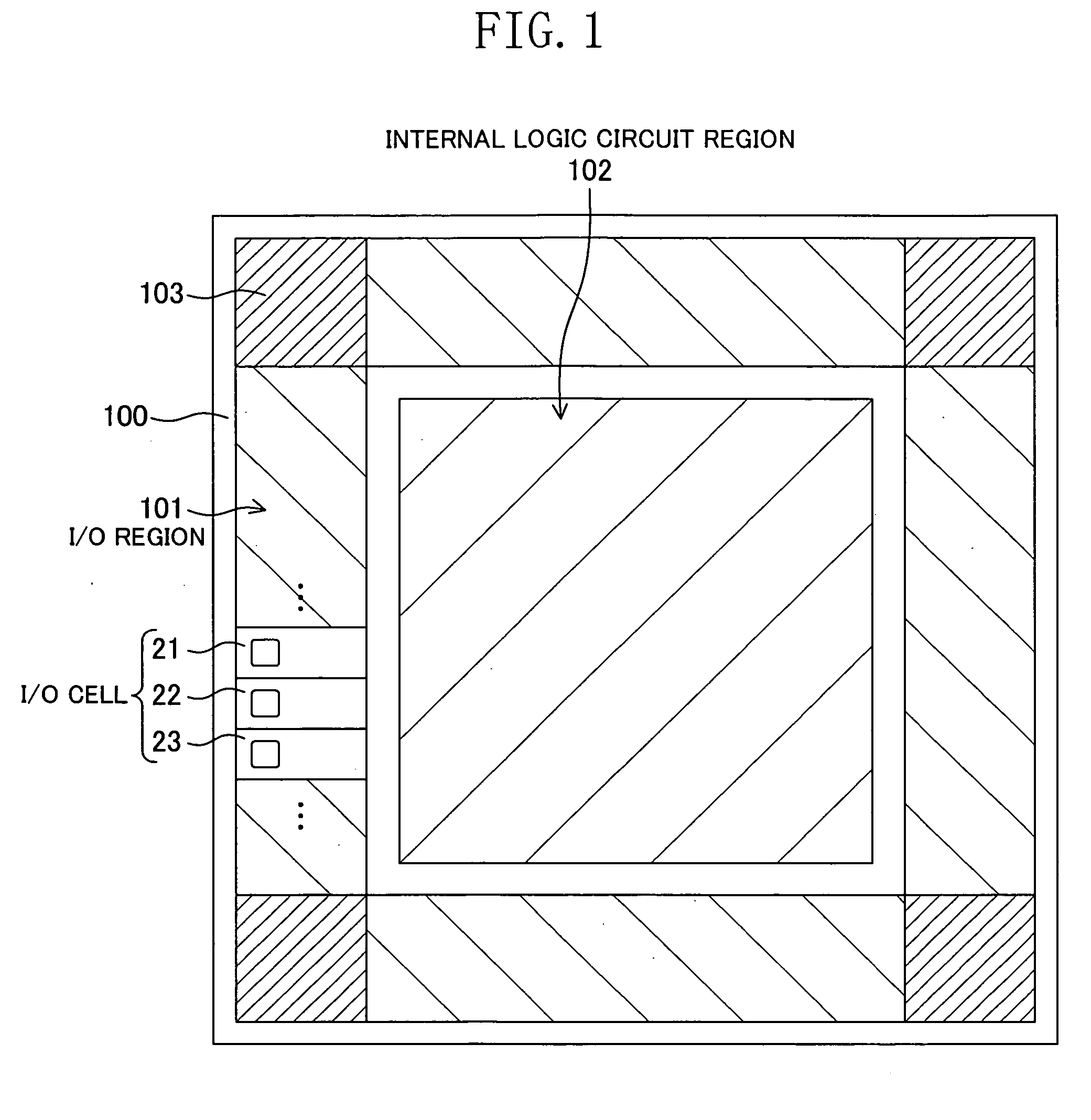
[0043] As described above, according to the present invention, a level shift circuit for a given I / O cell is placed in a given location outside the given I / O cell within the I / O region. Therefore, the area required for the given I / O cell can be reduced, and the pitch of I / O cells can be reduced. Thus, reduction in the area of the semiconductor chip having the necessary number of pins can be achieved.
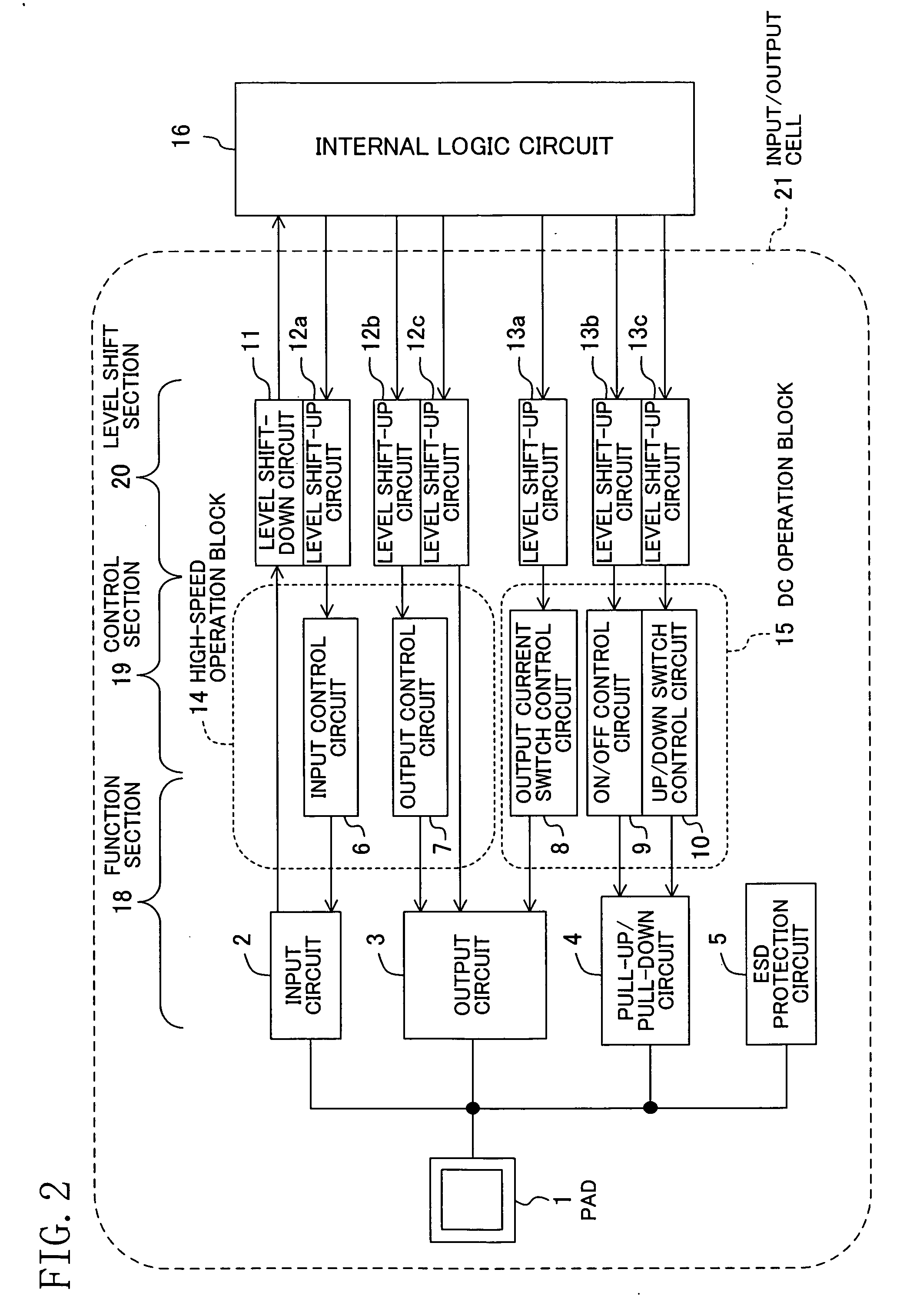
[0044] In particular, according to the present invention, a level shift circuit that is not asked for high-speed operation, that is, performs DC-like operation in which a given operation is maintained for a long time is selected as the level shift circuit to be placed outside the given I / O cell. Therefore, the high-speed operation of the internal logic circuit can be secured satisfactorily.
[0045] Moreover, according to the present invention, among control circuits to be provided for a given I / O cell, a control circuit that is connected to the level shift circuit placed outside the given I / O cell and is not asked for high-speed operation is also placed outside the given I / O cell. Therefore, the area required for the given I / O cell can further be reduced, and thus further reduction in the area of the semiconductor chip having the necessary number of pins can be achieved.

Problems solved by technology

As a result, the size of the semiconductor chip will be determined with the size of the I / O region, and this will cause disadvantages such as having wasteful space unused for placement of circuits in the internal logic circuit placement region.
However, this will also lead to increase in the area of the semiconductor chip, and thus should not be adopted.

Method used


Image

  • Semiconductor integrated circuit device and I/O cell for the same
  • Semiconductor integrated circuit device and I/O cell for the same
  • Semiconductor integrated circuit device and I/O cell for the same

Examples


embodiment 1

Alteration 1 to Embodiment 1

[0070]FIGS. 4A to 4D show Alteration 1 to Embodiment 1 described above.

[0071] In Embodiment 1, the three level shift circuits 13a to 13c for the input / output cell 21 were placed in the power supply cell 23. In this alteration, these three level shift circuits are placed in different locations.

[0072] Specifically, the three level shift circuits 13a to 13c for the input / output cell 21 are moved from the input / output cell 21 as shown in FIG. 4A, and placed in the dead spaces 26 of the input cell 22, the space cell 24 and the corner cell 25, respectively, as shown in FIGS. 4B, 4C and 4D. As a result, the input cell 22 has one level shift circuit 13a for fulfilling a function other than its own function, in addition to the function section 18, the high-speed operation block 14 and two level shift circuits 11 and 12a for fulfilling its own function. Likewise, the space cell 24 and the corner cell 25 respectively have the level shift circuits 13b and 13c for f...

embodiment 2

Alteration 2 to Embodiment 2

[0083]FIG. 7 shows Alteration 2 to Embodiment 2 of the present invention.

[0084] In this alteration, as shown in FIG. 7, common lines 39a to 39c are placed to run above the I / O region 101 for distributing the signals from the level shift circuits 13a to 13c.

[0085] With the configuration described above, in this alteration, the signal wiring region between the internal logic circuit 16 and the I / O region 10 can be reduced, and yet reduction in the area of the I / O region 101 can be achieved.

Embodiment 3

[0086] Embodiment 3 of the present invention will be described with reference to FIGS. 8A and 8B.

[0087] In Embodiment 1, the three level shift circuits 13a to 13c for the input / output cell 21 were placed outside the input / output cell 21, as shown in FIGS. 3A and 3B. In this embodiment, in addition to the three level shift circuits 13a to 13c, the DC operation block 15 connected to these level shift circuits 13a to 13c is also placed outside the input / outp...

embodiment 3

Alteration 1 to Embodiment 3

[0090]FIGS. 9A to 9D show Alteration 1 to Embodiment 3 of the present invention.

[0091] This alteration corresponds to FIGS. 4A to 4D showing Alteration 1 to Embodiment 1, in which the output current switch control circuit 8, the pull-up / pull-down ON / OFF control circuit 9 and the pull-up / pull-down switch control circuit 10 of the DC operation block 15 are respectively placed in the input cell 22, the space cell 24 and the corner cell 25.

Embodiment 4

[0092]FIG. 10 shows Embodiment 4 of the present invention.

[0093] In a semiconductor integrated circuit of FIG. 10, the DC operation blocks 15, 15 of the two input / output cells 21A and 21B are placed outside the input / output cells 21A and 21B, together with the level shift circuits 13a to 13b.

[0094]FIG. 10 corresponds to FIG. 5 showing the semiconductor integrated circuit device of Embodiment 2, but is different from FIG. 5 in that the DC operation blocks 15, 15 of the two input / output cells 21A and 21B are ...


PUM


Abstract

In a semiconductor integrated circuit device in which a plurality of I/O cells having level shift circuits are placed in an I/O region, two input/output cells respectively have four level shift circuits 11, 12a to 12c. A power supply cell, originally including only wiring for supply of a power supply voltage or a ground voltage, is additionally provided with three level shift circuits, which should originally be placed in the two input/output cells. The level shift circuits in the power supply cell are circuits asked for no high-speed operation and shared by the two input/output cells. This reduces the size of the two input/output cells and reduces the pitch of the I/O cells, permitting a larger number of required pins in a smaller area.

Description

CROSS-REFERENCE TO RELATED APPLICATIONS [0001] This application claims priority under 35 U.S.C. §119(a) on Patent Application No. 2005-109106 filed in Japan on Apr. 5, 2005, the entire contents of which are hereby incorporated by reference. BACKGROUND OF THE INVENTION [0002] The present invention relates to a semiconductor integrated circuit device provided with level shift circuits for shifting the potential level of a signal input or output into / from an internal logic circuit from / to the outside. [0003] With the recent process scaling-down achievement, the power supply voltage for internal circuits of a semiconductor integrated circuit tends to be increasingly lowered. In systems such as electronic equipment, however, some semiconductor elements used in the systems still adopt the conventional power supply voltage. Therefore, in such a system, on the occasion of conducting transmission / reception of a signal between such a semiconductor element and a semiconductor integrated circui...

Claims


Application Information

Patent Timeline
Patent Type & Authority Applications(United States)
IPC IPC(8): G01R31/28
CPCH01L24/06H01L27/0251H01L2224/05554H01L2924/14H01L2924/00
Inventor USAMI, SHIROMATSUOKA, DAISUKE
Owner SOCIONEXT INC
Why Eureka
Try Eureka