
Semiconductor device and its fabrication method

a technology of semiconductor devices and gate insulating films, which is applied in the direction of semiconductor devices, basic electric elements, electrical equipment, etc., can solve the problems of difficult to control the threshold voltage, the band potential is flat, and the threshold voltage is difficult to control by conducting ordinary channel ion implantation

Inactive Publication Date: 2006-10-26
KK TOSHIBA
View PDF3 Cites 15 Cited by
  • Summary
  • Abstract
  • Description
  • Claims
  • Application Information

AI Technical Summary

Problems solved by technology

However, it is reported that when a high-k gate insulating film such as hafnium silicate is combined with a polysilicon (poly-Si) gate electrode, a flat band potential (Vfb) shifts and it is difficult to control a threshold by conducting ordinary channel ion implantation (refer to C. Hobbs et al., VLSI'03).
In the case of this method, the work function only becomes a vicinity of a mid-gap and it is difficult to control a threshold voltage.
It is difficult to realize a semiconductor device in which high-performance MOSFETs are integrated.

Method used


Image

  • Semiconductor device and its fabrication method
  • Semiconductor device and its fabrication method
  • Semiconductor device and its fabrication method

Examples


first example

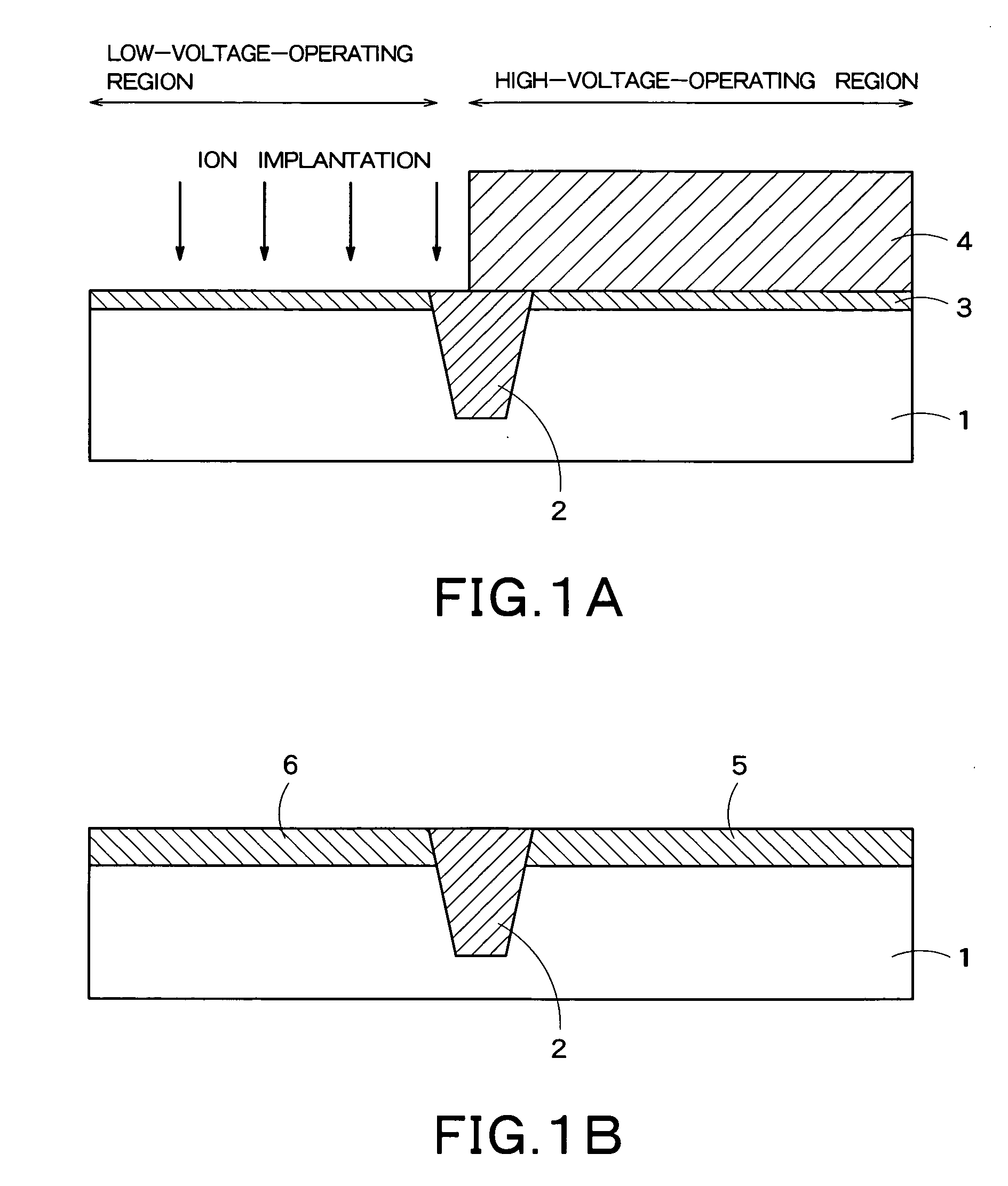
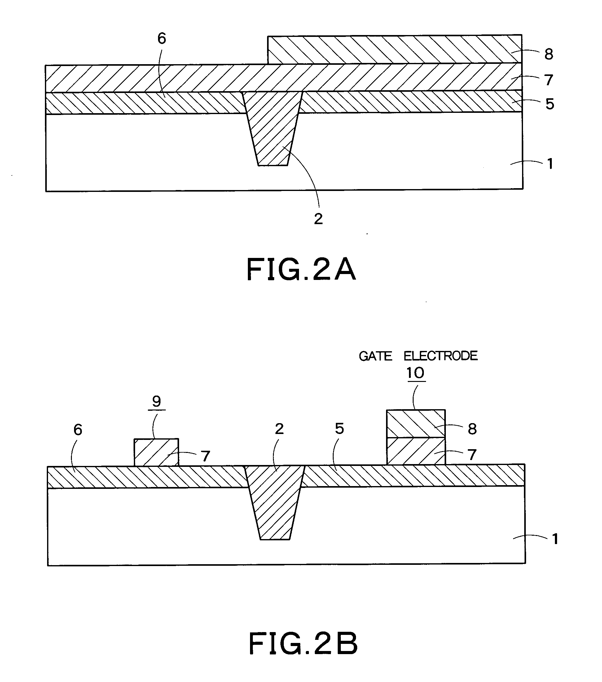
[0036] FIGS. 1 to 4 are sectional views for explaining the fabrication process of the semiconductor device according to first example of the present invention. First, a sacrifice oxide layer 3 having a thickness of 1 to 10 nm is formed by oxidation on a semiconductor substrate such as silicon on which a device separation region 2 such as STI (Shallow Trench Isolation) is formed on the surface area.

[0037] Then, a well region is formed and a threshold voltage is adjusted by performing ion implantation at a state of masking a predetermined device region with a photoresist 4 (FIG. 1A). Then, the sacrifice oxide film 3 is separated from the semiconductor substrate 1, heat treatment is applied to the semiconductor substrate 1 to form a silicon oxide film 5 having a thickness of 1 to 10 nm which serves as a gate insulating film. The silicon oxide film 5 becomes a thick gate insulating film for a high-voltage-operating MOSFET in a subsequent fabrication step. In this case, to decrease a ga...

second example

[0057] Second example described below is different from the first example in the structure of a high-voltage-operating MOSFET.

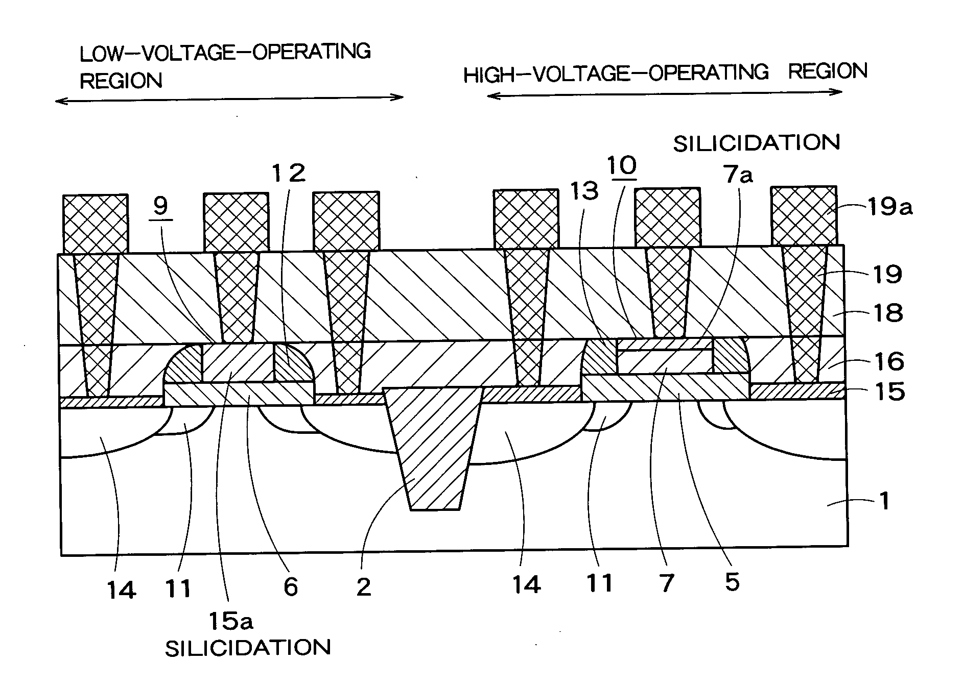
[0058]FIGS. 5A-5C are sectional views for explaining fabrication process of the semiconductor device according to the second example of the present invention. In the case of this example, polysilicon is used as the starting material of a gate electrode for a low-voltage-operating MOSFET and a film obtained by containing germanium in polysilicon is used for a high-voltage-operating MOSFET. Moreover, the whole gate electrode is silicided for the low-voltage-operating MOSFET but only a part of a gate electrode is silicided for the high-voltage-operating MOSFET.

[0059] This example is the same as the first example in steps of forming a plurality of gate insulating films and depositing the polysilicon film made of a gate electrode. A high-k film 26 such as hafnium silicon oxynitride (HfSiON) having a thickness of 0.1 to 10 nm serving as the gate insulating film i...

third example

[0068] A third example described below forms a MOSFET on an SOI substrate.

[0069]FIGS. 6A and 6B are sectional views for explaining a semiconductor device according to the third example of the present invention. In the case of the semiconductor device shown in FIG. 6A, the SOI substrate is provided in a low-voltage-operating region. A device separation region 32 such as STI is formed on the surface region of a semiconductor substrate 31 made of silicon or the like. A MOSFET (low-voltage-operating MOSFET) having a gate insulating film made of a high-k film is formed in a low-voltage-operating region on the SOI substrate and a MOSFET (high-voltage-operating MOSFET) having a gate insulating film made of a silicon oxide film is formed on the normal bulk substrate.

[0070] The SOI substrate in the low-voltage-operating region has an insulating layer 38 such as a silicon oxide film formed on the semiconductor substrate 31 and a silicon layer 41 formed on the insulating layer 38. A shallow ...


PUM


Abstract

A semiconductor device has a semiconductor substrate, a first MOSFET which has a first gate insulating film made of a high dielectric material formed above the semiconductor substrate and a first gate electrode formed above the first gate insulating film, an insulating film which is formed directly on sidewalls of the first gate electrode and made of a material having dielectric constant smaller than that of the first gate insulating film, and a second MOSFET which has a second gate insulating film made of a material having dielectric constant smaller than that of the first gate insulating film formed above the semiconductor substrate and a second gate electrode formed above the second gate insulating film, wherein the first gate electrode is formed of a first silicide or a first metal; and the second gate electrode is formed including a film made of at least one of polysilicon, amorphous silicon, polysilicon germanium and amorphous silicon germanium.

Description

CROSS REFERENCE TO RELATED APPLICATIONS [0001] This application is based upon and claims the benefit of priority from the prior Japanese Patent Application No. 2005-56971, filed on Mar. 2, 2005, the entire contents of which are incorporated herein by reference. BACKGROUND OF THE INVENTION [0002] 1. Field of the Invention [0003] The present invention relates to a gate electrode and a gate insulating film of a semiconductor device such as a MOSFET. [0004] 2. Related Art [0005] In a MOSFET used for a semiconductor device such as an LSI, device size tends to be miniaturized in order to realize high integration of the devices, low cost and high performance. A thickness of a gate insulating film is also scaled down in the same way. However, when a physical film thickness indicating an actual thickness becomes 2 nm or less, current flows from a gate electrode through a substrate due to a tunnel phenomenon. To decrease the gate leak current, it is necessary to increase the physical film thi...

Claims


Application Information

Patent Timeline
IPC IPC(8): H01L27/12
CPCH01L21/823443H01L27/1203H01L21/823462H01L21/82345
Inventor ISHIMARU, KAZUNARI
Owner KK TOSHIBA
Learn More