Spin injection magnetic domain wall displacement device and element thereof

a magnetic domain wall and displacement device technology, applied in the direction of magnetic bodies, instruments, transportation and packaging, etc., can solve the problems of increasing thermal fluctuation, random displacement of the position of the magnetic domain wall by thermal agitation, and inability to keep the magnetization of the recording cell

Inactive Publication Date: 2006-10-26
FUJI ELECTRIC CO LTD
View PDF25 Cites 43 Cited by
  • Summary
  • Abstract
  • Description
  • Claims
  • Application Information

AI Technical Summary

Benefits of technology

[0018] In one embodiment, the third magnetic layer group comprises a nonmagnetic intermediate exchange coupling control layer, an intermediate ferromagnetic layer, a nonmagnetic third exchange coupling control layer, and the third ferromagnetic layer laminated together in this order. The intermediate exchange coupling control layer is in contact with the magnetic domain wall displacement layer.
[0019] In another embodiment, the third magnetic layer group comprises a nonmagnetic exchange coupling control layer and the third ferromagnetic layer laminated together. The exchange coupling control layer is in contact with the magnetic domain wall displacement layer.
[0020] The film thickness of the intermediate ferromagnetic layer is smaller than the spin relaxation length of electr

Problems solved by technology

For example, in the case of the MRAM shown in FIG. 12, when its volume and its saturation magnetization are made small, a problem arises in that thermal stability of recording bit, namely thermal stability of magnetization of the recording cell 109, is reduced, causing thermal fluctuation of magnetization by thermal disturbances, even at room temperature, making it impossible to keep the magnetization of the recording cell.
However, lowering the magnetization saturatio

Method used


Image

  • Spin injection magnetic domain wall displacement device and element thereof
  • Spin injection magnetic domain wall displacement device and element thereof
  • Spin injection magnetic domain wall displacement device and element thereof

Examples


first embodiment

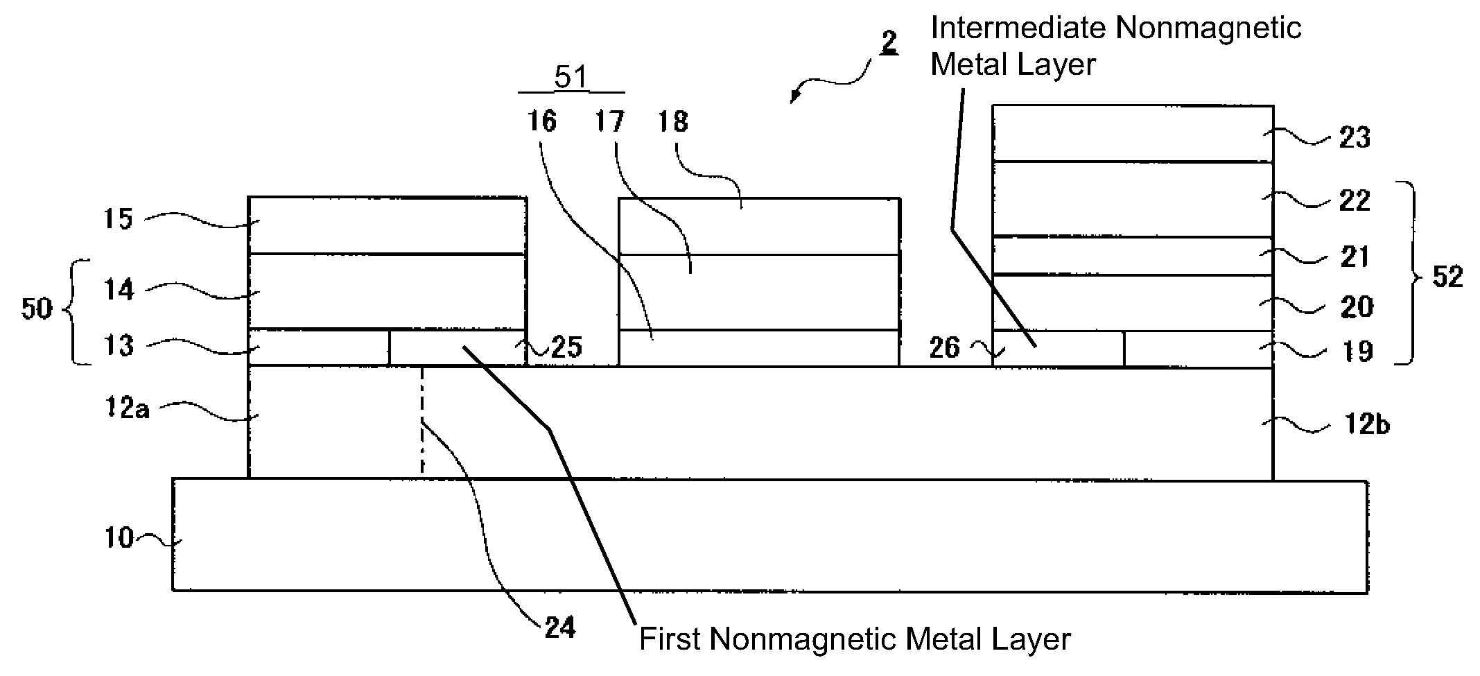
[0042]FIG. 1 is a schematic cross sectional view for explaining an example of the basic arrangement of a spin injection magnetic domain wall displacement element 1 according to the invention. On a substrate 10, a magnetic domain wall displacement layer 12 is formed. First, second, and third magnetic layer groups 50, 51, 53 are formed in this order on one side of the magnetic domain wall displacement layer 12. The first magnetic layer group 50 is formed on one end of the magnetic domain wall displacement layer 12 and a first electrode 15 is formed on the first magnetic group 50. On the other end of the magnetic domain wall displacement layer 12, the third magnetic layer group 52 is formed and a third electrode 23 is formed on the third magnetic layer group 52. At a position between the first magnetic layer group 50 and the third magnetic layer group 52, the second magnetic layer group 51 is formed on the magnetic domain wall displacement layer 12 and a second electrode 18 is formed o...

second embodiment

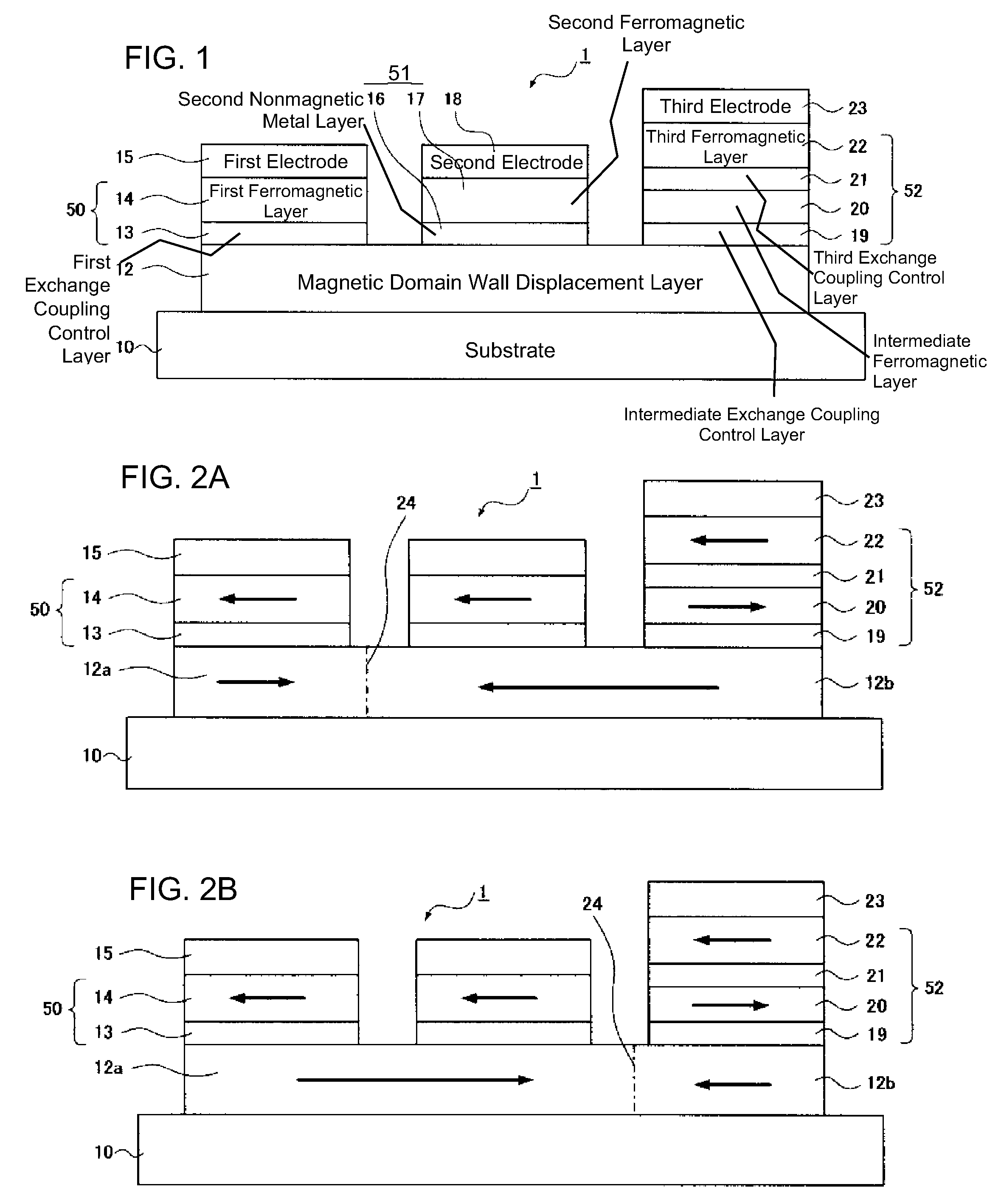
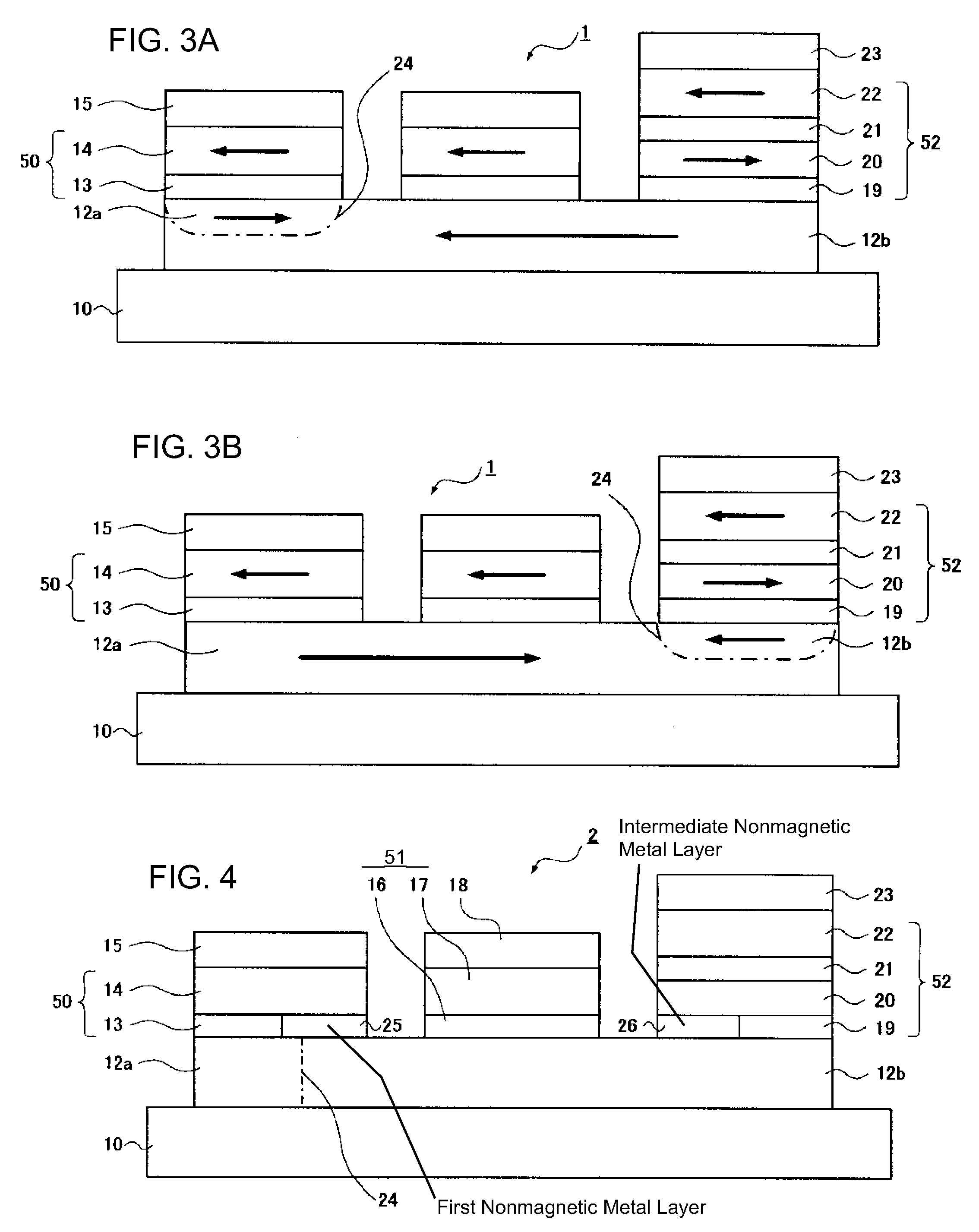
[0078]FIGS. 6A and 6B are schematic cross sectional views for explaining the operation principle of the example of the arrangement of the element of the second embodiment according to the invention. In each of the magnetic layers in the element shown in FIG. 5, the direction of magnetization thereof is shown with an arrow. The magnetic domain wall displacement layer 12 is divided by a magnetic domain wall 24 into the magnetic domain wall displacement layer 12a on the first electrode 15 side and the magnetic domain wall displacement layer 12b on the third electrode 23 side. The arrangement shown in FIG. 5 is the minimum unit of the element and the necessary number of the elements disposed on the same substrate to form a desired device. Circuits and driving elements for driving the elements according to the invention can be also arranged on the same substrate.

[0079] The substrate 10, the first electrode 15, the first ferromagnetic layer 14, the first exchange coupling control layer 13...


PUM


Abstract

A spin injection magnetic domain wall displacement device has a plurality of spin injection magnetic domain wall displacement elements. Each element includes a magnetic domain wall displacement layer having a magnetic domain wall, and a first, second, and third magnetic layer groups each having a ferromagnetic layer. The first, second, and third magnetic layer groups are disposed in the order on the same side of the magnetic domain wall displacement layer. The magnetic domain wall is displaceable by flowing electrons between the first and third magnetic layer groups. The position of the magnetic domain wall in the magnetic domain wall displacement layer is detectable based on the difference in the electrical resistance across the second and first or third magnetic layer groups. The magnetic domain wall displacement layer is in antiferromagnetic coupling with the first magnetic layer group, and in antiferromagnetic or ferromagnetic coupling with the third magnetic layer group. The element enables detection of displacement of the magnetic domain wall by measuring the change in the electric resistance.

Description

BACKGROUND [0001]FIG. 10 schematically shows a cross sectional structure for explaining an example of an arrangement of a previously proposed GMR (Giant Magneto-Resistance) element making use of a GMR effect. For example, on a silicon substrate 100, a lower electrode 101, a lower ferromagnetic layer 103 (with a thickness of approximately 40 nm and a diameter of approximately 100 nm) made of a material such as Co, a nonmagnetic metal layer 104 (with a thickness of approximately 6 nm and a diameter of approximately 100 nm), an upper ferromagnetic layer 105 (with a thickness of approximately 2.5 nm and a diameter of approximately 100 nm) made of a material such as Co, and an upper electrode 106 are formed in this order. Further, a bit line 102 is formed on the lower electrode 101. It is known that such a GMR structure element can reverse the direction of magnetization of the upper ferromagnetic layer 105 by spin current injection from the upper electrode 106 side, that is, injection of...

Claims


Application Information

Patent Timeline
IPC IPC(8): G11B5/39H01L43/00G11B5/33H01L29/82
CPCG11C11/16G11C19/0808Y10T428/1193H01L43/08Y10T428/1121H01F10/3272H10N50/10
Inventor SAITO, AKIRA
Owner FUJI ELECTRIC CO LTD
Why Eureka
Try Eureka