Image sensor and control method of the image sensor

a control method and image sensor technology, applied in the field of image sensors, can solve the problems of affecting the operation speed of the counter 105, affecting the quality of the image sensor, and becoming difficult to apply the image sensor having such an a/d converter to products requiring high speed operation, etc., to achieve high accuracy, high resolution, and high speed

Active Publication Date: 2006-11-02
DENSO CORP
View PDF3 Cites 74 Cited by
  • Summary
  • Abstract
  • Description
  • Claims
  • Application Information

AI Technical Summary

Benefits of technology

[0018] It is an object of the present invention to provide a new and improved image sensor of a small size formed in a single IC chip, on which a light receiving element array and an A / D conversion circuit are formed. The image sensor of the present invention is capable of executing a high speed processing such as zoom-in (zoom-up) function with high accuracy and a high resolution.

Problems solved by technology

However, the conventional image sensor 100 having the configuration disclosed by the Japanese patent laid open publication number JP2000-349638 cannot perform the A / D conversion only for the target 2D part of the image.
However, the fast counting of the counter 105 involves a limitation in operation.
Further, decreasing the slope of the lamp wave requires a long processing time for the A / D conversion, and it is thereby difficult to apply the image sensor having such an A / D converter to products requiring a high speed operation.
Because the number of bits of the counter has a limitation of approximately 10 bits, it becomes difficult to apply such a conventional image sensor to products requiring a high resolution.

Method used


Image

  • Image sensor and control method of the image sensor
  • Image sensor and control method of the image sensor
  • Image sensor and control method of the image sensor

Examples


first embodiment

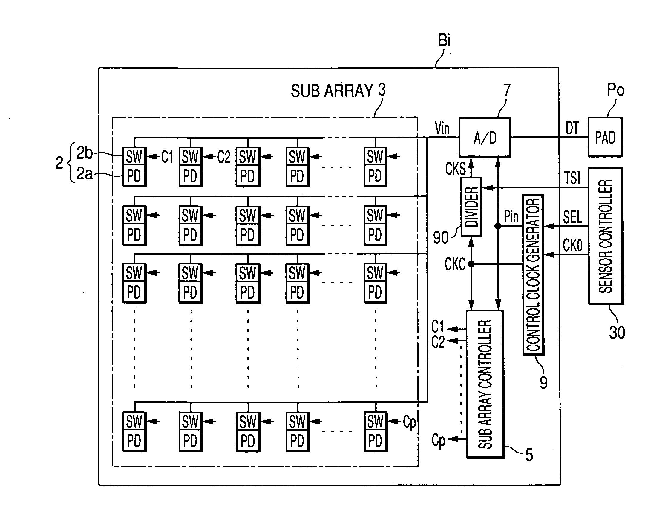
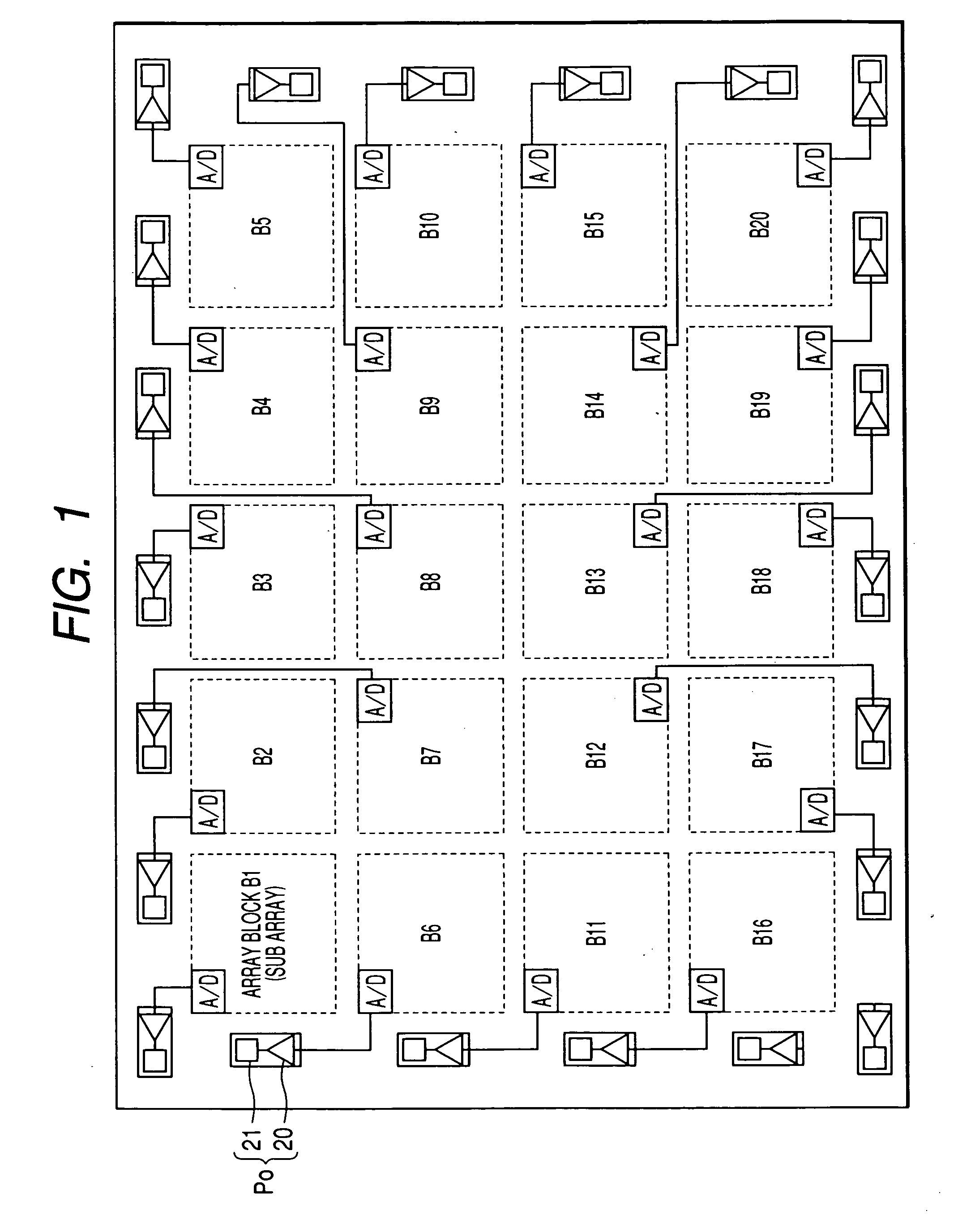
[0037]FIG. 1 is a block diagram showing a configuration of an image sensor 1 according to the first embodiment of the present invention. In particular, FIG. 1 shows an arrangement of plural array blocks Bi (i=1 to 20 in the embodiment) arranged in matrix form and peripheral units in the image sensor 1 of the first embodiment. The peripheral units are output pads Po and plural pads (not shown). Each array block Bi has the corresponding output pad Po. Through the plural pads (not shown), signals of various types excepting the output signals transferred through the output pads Po are input and output. The output signal from each array block Bi (i=1 to 20) is transferred through the corresponding output pad Po. As shown in FIG. 1, those output pads Po and the other plural pads are formed at the peripheral area of the array block, that is, formed at the peripheral section of the IC chip. Although FIG. 1 shows only one transfer line through which the output pad Po and each array block Bi ...

second embodiment

[0086] Next, a description will now be given of the image sensor according to the second embodiment of the present invention. The difference between the first embodiment and the second embodiment is the data collection in the zoom-in process (or zoom-up process).

[0087]FIG. 7 is a flow chart showing the process of the zoom-in data collection in the image sensor according to the second embodiment of the present invention.

[0088] First, target array blocks Bi to be processed and the number “n” of the target array blocks Bi are specified based on a zoom-in instruction signal supplied from an external device of the array block Bi such as the sensor controller 30 (step S210).

[0089] Based on the total number “m” of the array blocks Bi and the number “n” of the target array blocks specified in step S210, an iteration number “k” (=[m / n]) is calculated and a variable “j” is initialized to 1 (step S220), where [x] means an integer part of the value “x”.

[0090] Following, the variable “i” for...

third embodiment

[0103] Next, a description will now be given of the image sensor of the third embodiment according to the present invention with reference to FIG. 8.

[0104]FIG. 8 is a block diagram showing a configuration of an A / D conversion circuit (also showing a part of a circuit diagram) in an array block in the image sensor according to the third embodiment. The difference between the third embodiment and the first embodiment is the configuration of the A / D conversion circuit. Other components of the third embodiment are the same of those of the first embodiment.

[0105] As shown in FIG. 8, a delay unit DU of an initial stage forming a pulse delay circuit 10a that forms an A / D conversion circuit 7a in the image sensor of the third embodiment is made of an AND gate DUa. The input pulse Pin as an initiation signal is input to one input terminal of the AND gate DUa. Another input terminal of the AND gate DUa is connected to the output terminal of the delay unit DU of the final stage. Thus, all of...


PUM


Abstract

An image sensor has plural array blocks B1 to B20 arranged in a two dimensional (2D) arrangement. Each array block has a sub array and a corresponding analogue to digital (A/D) converter for performing an A/D conversion of light signals (or detection signals) output from the sub array. The sub array has plural picture element cells arranged in a 2D arrangement. Each A/D converter has a pulse delay circuit having delay units of plural stages connected in series. Each delay unit delays an input pulse by a delay time corresponding to a level of the light signals received from the sub array. A pulse delay type A/D converter is used as the A/D converter, which outputs the number of the delay units as an A/D conversion data item through which the input pulse passes for a measurement time period.

Description

CROSS-REFERENCE TO RELATED APPLICATIONS [0001] This application is related to and claims priority from Japanese Patent Application No. 2005-108824 filed on Apr. 5, 2005, the contents of which are hereby incorporated by reference. BACKGROUND OF THE INVENTION [0002] 1. Field of the Invention [0003] The present invention relates to an image sensor of a single IC chip and a control method of the image sensor having a light receiving element array arranged in a two dimensional (2D) arrangement and a plurality of analogue to digital (A / D) conversion circuits. The light receiving element array has at least picture element cells made of photoelectric conversion elements arranged in a 2D array, and the A / D conversion circuits perform A / D conversion of detection signals or light signals transferred from the light receiving element array. [0004] 2. Description of the Related Art [0005] Recently, there is a strong demand to provide an image sensor capable of performing a high speed operation an...

Claims


Application Information

Patent Timeline
Patent Type & Authority Applications(United States)
IPC IPC(8): H01L27/00H03M1/12H03M1/50H04N5/335H04N5/341H04N5/369H04N5/374H04N5/376H04N5/378
CPCH04N3/1593H04N3/155H04N25/772H04N25/41
Inventor WATANABE, TAKAMOTO
Owner DENSO CORP
Why Eureka
Try Eureka