With a nitride semiconductor element, sapphire is often used for the substrate, but it becomes difficult to reduce the cost of the nitride semiconductor element when sapphire is used for the substrate, since sapphire is high in cost.
Furthermore, since sapphire is an insulator, if it is used as the substrate, instead of providing electrodes on the rear surface of the substrate, it becomes necessary to
expose a portion of the nitride semiconductor layer above the substrate, and to form the electrodes on this exposed portion (when this is done, the area of the nitride semiconductor element becomes greater, and it becomes difficult to reduce the cost).
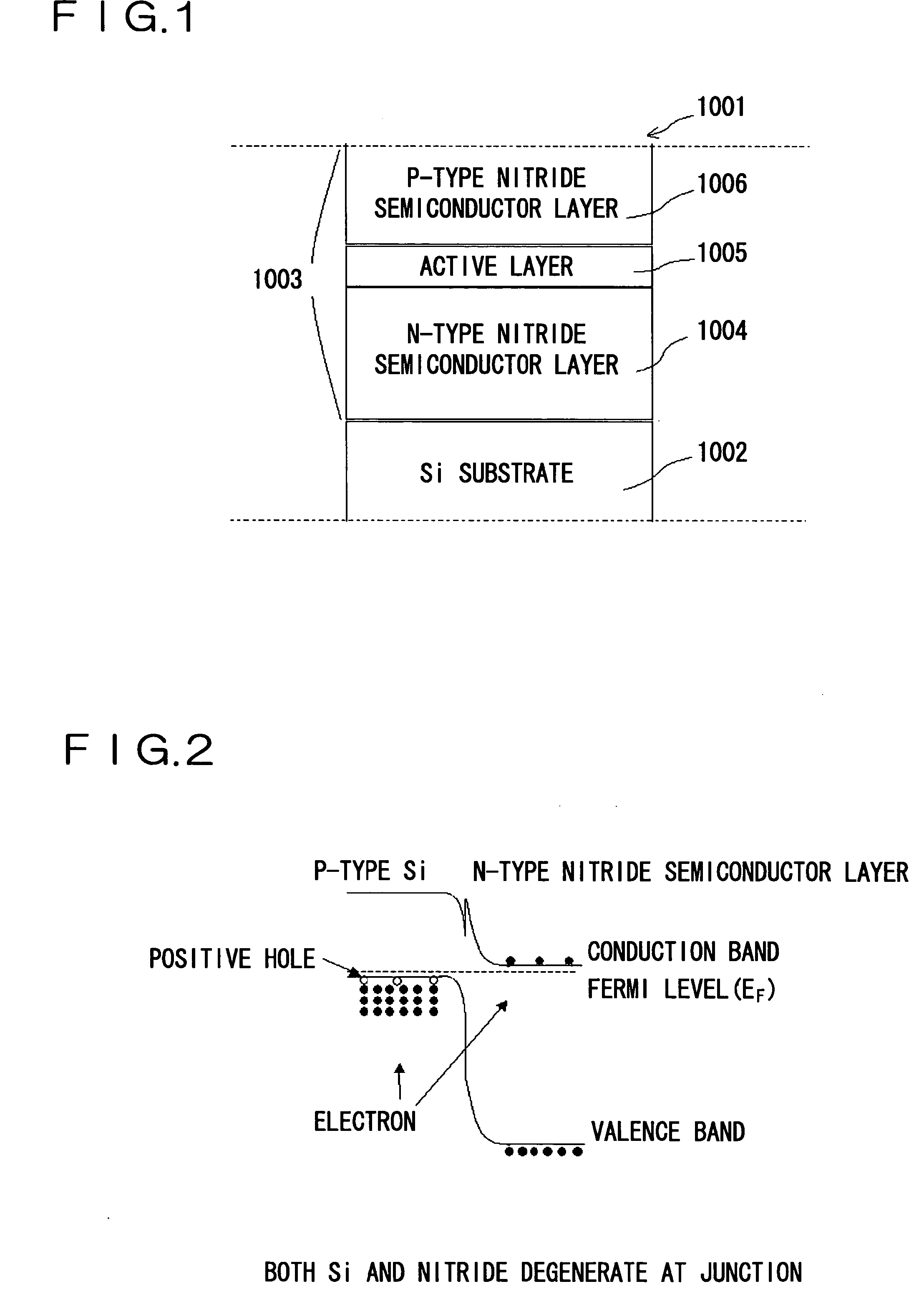
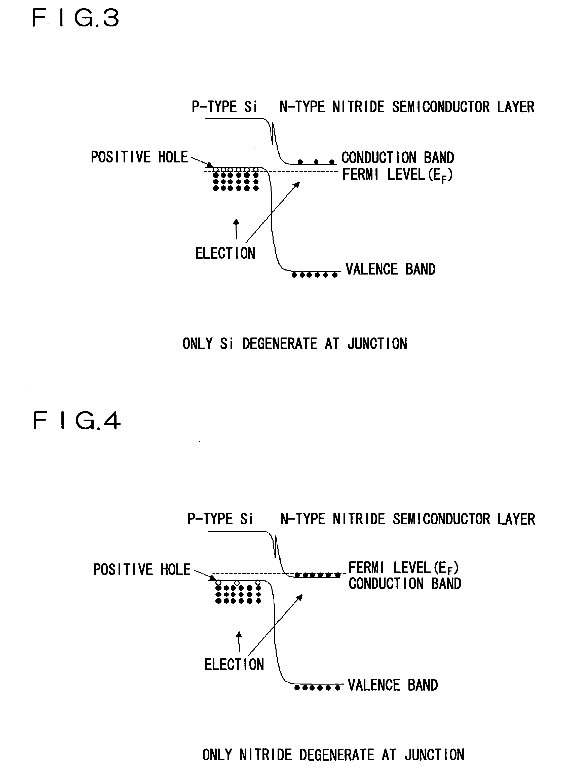
However, in Japanese Patent Laid-Open Publication 2003-179258, Japanese Patent Laid-Open Publication 2003-142729, and Japanese Patent Laid-Open Publication 2003-8061, with an Si substrate and a nitride semiconductor layer, it is considered that, at their junction as shown in FIG. 24, a high electrical potential barrier is present at the interface between them; and accordingly, with the above described nitride semiconductor element, there has been the problem that the
voltage (Vf) in the forward direction is extremely high.
Furthermore although, as in Japanese Patent Laid-Open Publication 2000-004047 etc., there is a method of providing a LED element by forming a diffuse layer or the like on an Si substrate, and by making a light receiving element or the like by forming a p-n junction and by laminating it on this substrate, however, with these hetero-junction interfaces between the Si substrate and the
compound semiconductor of the LED element, it is not possible to implement a junction which is appropriate for the operation of the element, so that it has been difficult to drive both of the elements (the Si substrate and the LED element) sufficiently.
In concrete terms, with these hetero-junction interfaces, it becomes difficult to plan sufficient matching for the bands etc., due to the
band offset at these interfaces, and moreover when bias is applied.
Furthermore, when growing a GaN type semiconductor on several different types of material surfaces, problems arise of crystalline deterioration due to non-matching of the lattices, differences in the coefficients of
thermal expansion, and the like, so that, due to this as well, the above described problems at the junction portions between the different types of material are promoted and become worse.
In addition, when the Si
substrate surface at the junction portion with the GaN layer is an
impurity diffusion region or the like, that region undergoes crystalline deterioration, and it is considered that the problems like those described above in growing the GaN layer thereon become yet more acute at the hetero-junction interface.
In Japanese Patent Laid-Open Publication Heisei 11-224958, a device is proposed in which a LED element structure is formed from a
SiC substrate, a SiC layer thereover, and a GaN type layer over that; but, since a p-n junction made with an interface between different materials is provided within this LED structure, a barrier occurs between the bands at this hetero-material interface, so that it is difficult to obtain a satisfactory LED element.
In Japanese Patent Laid-Open Publication 2000-031535 it is proposed, in order to form a light emitting element structure with a GaN type semiconductor on a Si substrate, to interpose various different types of material (BP, ZnO, SiO2), but the same type of problem as that described above occurs, since this material has a hetero-junction interface with both the Si substrate and the GaN layer.
Furthermore, with the buffer of Japanese Patent Laid-Open Publication 2002-170776, the crystalline characteristics of the nitride semiconductor layer which is formed on the Si substrate do not become adequate.
Furthermore, in particular, if a nitride semiconductor layer is formed on a Si substrate, there is a tendency for it to be difficult to obtain a nitride semiconductor layer of good crystalline characteristics.
Due to this, with the
superlattice structure of the above described Japanese Patent Laid-Open Publication 2002-170776, in the case of forming, in particular, a nitride semiconductor layer while using a Si substrate as the substrate, it is the current situation that it is not possible to obtain a nitride semiconductor layer whose crystalline characteristics are as good as before.
With the above described integrated element, for example in Japanese Patent Laid-Open Publication Heisei 7-321051, in order to arrange a LED portion and a MOS portion within the surface of the substrate, the manufacturing cost becomes high, since the area per one element becomes large.
On the other hand, with such an element which is integrated within the
substrate surface, since there is a necessity for wiring up each element portion, a lot of man-hours are required, and the manufacturing cost is also increased thereby.
Furthermore, since the
area ratio which is occupied by the light emitting portion within the surface is low, when implementing a
light emitting device or the like, the size of the light emitting portion is small in comparison with the implementation area for the element, so that it is difficult to obtain a satisfactory light output.
Yet further, in order to arrange the LED portion and the MOS portion within the surface of the substrate, limitations arise with regard to the position of the LED within the surface of the element, in other words with regard to the position of the
light source, and, in the implementation of a
light emitting device or the like, position adjustment of a
point light source becomes difficult, and in addition the optical design of the reflecting plate for the
light emitting device becomes difficult, so that it is difficult to obtain a light emitting device with a suitable light output.
On the other hand, as another example of the above described integrated element, there is a method, as described in Japanese Patent Laid-Open Publication 2000-004047 etc., of making a p-n junction by diffusing a layer into a Si substrate, and thereby forming a light receiving element or the like, and of laminating on this substrate, thus providing a LED element; but it is not possible to implement an appropriate junction for element operation at the hetero-junction interface between the Si substrate and the semiconductor compound of the LED element, and it has been difficult to drive each of the elements (the Si substrate and the LED element) sufficiently.
In concrete terms, with a hetero-junction interface, it becomes difficult to plan on sufficient matching of the
band offset and so on at this interface, and further to plan for sufficient matching of the bands etc. when they are biased.
According to considerations by the present inventors, since, as shown in FIG. 25, at the junction between the Si substrate and the nitride semiconductor layer, a high electrical potential barrier is present between both of them where they are joined (i.e. at the interface), it has been realized that there is a problem, in the above described prior art type of nitride semiconductor element which uses a Si substrate, with regard to the fact that the
voltage in the forward direction (Vf) is extremely high.
Furthermore, since they are integrated within the surface, in the same way as described above, there are problems with regard to light output, and with regard to the implementation and the manufacturing cost of such a light emitting device.
In Japanese Patent Laid-Open Publication Heisei 11-224958, it is proposed to form a LED element structure from a
SiC substrate, a SiC layer over it, and a GaN type layer over that; but, since a hetero-material interface is provided within this LED structure, a barrier between bands occurs at the above described hetero-material interface, and it is difficult to obtain a suitable LED element.

