MOS or CMOS sensor with micro-lens array

a micro-lens array and sensor technology, applied in the direction of electrical equipment, semiconductor devices, radio frequency controlled devices, etc., can solve the problems of high rail-to-rail voltage swing, large energy consumption of ccd sensors, and problems of today's mobile appliances, so as to minimize or eliminate pixel-to-pixel crosstalk, increase the electrical resistivity in the bottom layer, and reduce the effect of pixel-to-pixel crosstalk

Inactive Publication Date: 2006-11-09
E PHOCUS
View PDF1 Cites 116 Cited by
  • Summary
  • Abstract
  • Description
  • Claims
  • Application Information

AI Technical Summary

Benefits of technology

[0008] The present invention provides a MOS or CMOS sensor with a multi-layer photodiode layer covering an array of active pixel circuits. The multi-layer photodiode layer of each pixel is fabricated as continuous layers of charge generating material on top of the MOS and/or CMOS pixel circuits so that extremely small pixels are possible with almost 100 percent packing factors. The sensor includes special features to minimize or eliminate pixel to pixel crosstalk. A micro-lens array with a micro-lens positioned above each pixel directs light illuminating the pixel toward the central portion of the pixel and away from its edges. Also, preferably carbon is added to doped amorphous silicon N or P bottom layer of the multi-layer photodiode layer to increase the electrical resistivity in the bottom layer to further discourage crosstalk. In preferred embodiments each of the pixels define a ti...

Problems solved by technology

One big drawback with CCD's is that the technique for producing CCD's is incompatible with other integrated circuit technology such as MOS and CMOS technology, so that processing circuits and the CCD arrays must be produced on chips separate from the CCD's.
Another drawback is that the CCD sensors consume large amounts of energy (as compared to cameras with CMOS sensors) and require high rail-to-rail voltage swings to operate CCD.
This can pose problems for today's mobile appliances, such as Cellular Phone and Personal Digital Assistant.
The active circuitry consists of multiple transistors that are inter-connected by metal lines; as a result, this area is opaque to visible light and cannot be used for photo-sensing.
Small cameras using CMOS sensors typically use less energy than CCD sensors an...

Method used


Image

  • MOS or CMOS sensor with micro-lens array
  • MOS or CMOS sensor with micro-lens array
  • MOS or CMOS sensor with micro-lens array

Examples


Embodiment Construction

[0024] In the following description of preferred embodiments, reference is made to the accompanying drawings, which form a part hereof, and which show by way of illustration a specific embodiment of the invention. It is to be understood by those of working skill in this technological field that other embodiments may be utilized, and structural, electrical, as well as procedural changes may be made without departing from the scope of the present invention.

Need to Avoid Crosstalk

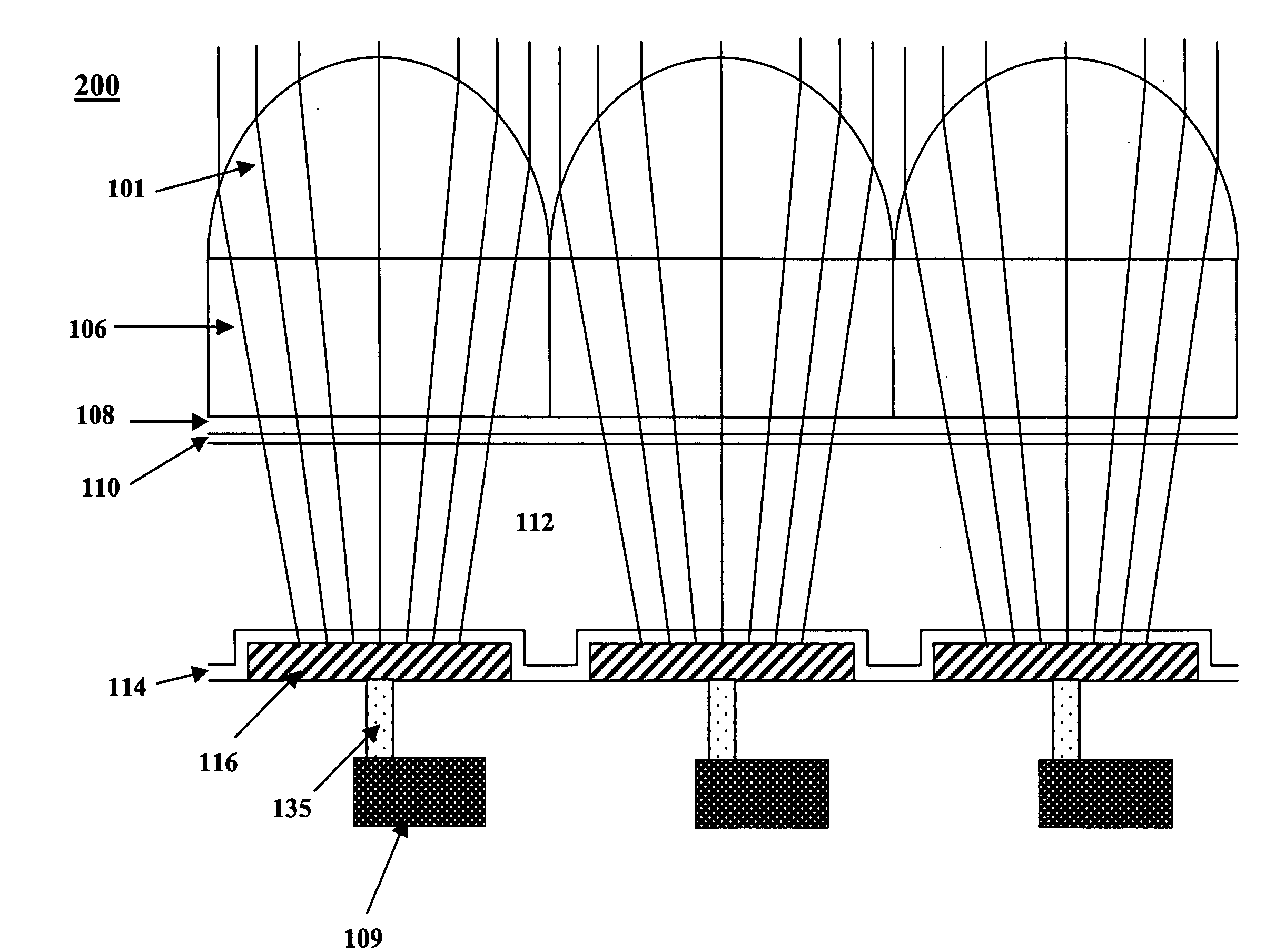
[0025] CMOS sensors having a multi-layer photodiode layer covering an array of active pixel circuits are described in detail in the parent patent applications listed in the first sentence of this specification. This architecture permits pixel designs with extremely small pixels (measured in microns) with almost 100 percent packing factors. A potential problem with this architecture is the possibility of crosstalk. Charges generated above a particular pixel circuit in the multilayer photodiode layer can be dr...


PUM


Abstract

A MOS or CMOS sensor with a multi-layer photodiode layer covering an array of active pixel circuits. The multi-layer photodiode layer of each pixel is fabricated as continuous layers of charge generating material on top of the MOS and/or CMOS pixel circuits so that extremely small pixels are possible with almost 100 percent packing factors. The sensor includes special features to minimize or eliminate pixel to pixel crosstalk. A micro-lens array with a micro-lens positioned above each pixel directs light illuminating the pixel toward the central portion of the pixel and away from its edges. Also, preferably carbon is added to doped amorphous silicon N or P bottom layer of the multi-layer photodiode layer to increase the electrical resistivity in the bottom layer to further discourage crosstalk. In preferred embodiments each of the pixels define a tiny surface area equal to or larger than about 3.24 square microns and smaller than or equal to about 25 square microns. Detailed descriptions are provided for two general types of sensors. The first type has a pixel count of about 0.3 to 1.9 million pixels and are especially suited for sues such as cell phone cameras. The second type with pixel count of between about 1.9 million pixels to more than 5 million pixels is especially suited for high definition television cameras.

Description

FIELD OF THE INVENTION [0001] This application is a continuation in part of U.S. patent applications Ser. No. 11 / 361,426 filed Feb. 24, 2006, Ser. No. 11 / 389,356 filed Mar. 24, 2006 and Ser. No. 10 / 921,387, filed Aug. 18, 2004 which is a continuation in part of Ser. Nos. 10 / 229,953 filed Aug. 27, 2002; 10 / 229,954 filed Aug. 27, 2002 (now U.S. Pat. No. 6,791,130); 10 / 229,955 filed Aug. 27, 2002; 10 / 229,956 filed Aug. 27, 2002, (now U.S. Pat. No. 6,798,033); 10 / 648,129 filed Aug. 26, 2003, (now U.S. Pat. No. 6,809,358); 10 / 746,529 filed Dec. 23, 2003. Ser. No. 10 / 648,129 was a continuation in part of Ser. No. 10 / 072,637 filed Feb. 5, 2002 (now U.S. Pat. No. 6,730,914 and Ser. No. 10 / 371,618 filed Feb. 22, 2003 (now U.S. Pat. No. 6,730,900). All of the above patents and patent applications are hereby incorporated herein by reference. The present invention relates to cameras and in particular to cameras with MOS or CMOS sensors.BACKGROUND OF THE INVENTION [0002] Electronic image sensors...

Claims


Application Information

Patent Timeline
IPC IPC(8): H01L31/113
CPCH01L27/14609H01L27/14621H01L27/14627H01L27/14632H01L27/14692H01L27/14645H01L27/14685H01L27/14687H01L27/14636
Inventor HSIEH, TZU-CHIANG
Owner E PHOCUS
Why Eureka
Try Eureka