

Insulating film measuring device, insulating film measuring method, insulating film evaluating device, insulating film evaluating method, substrate for electric discharge display element, and plasma display panel
a technology of insulating film and measuring method, which is applied in the manufacture of electric discharge tubes/lamps, instruments, electrode systems, etc., can solve the problem that the coefficient is not necessarily appropriate for accurately evaluating the discharge characteristics of a pdp, and achieves the effect of improving yield and the like, and obtaining information simply and accurately
- Summary
- Abstract
- Description
- Claims
- Application Information
AI Technical Summary
Benefits of technology
Problems solved by technology
Method used
Image

Examples
first embodiment
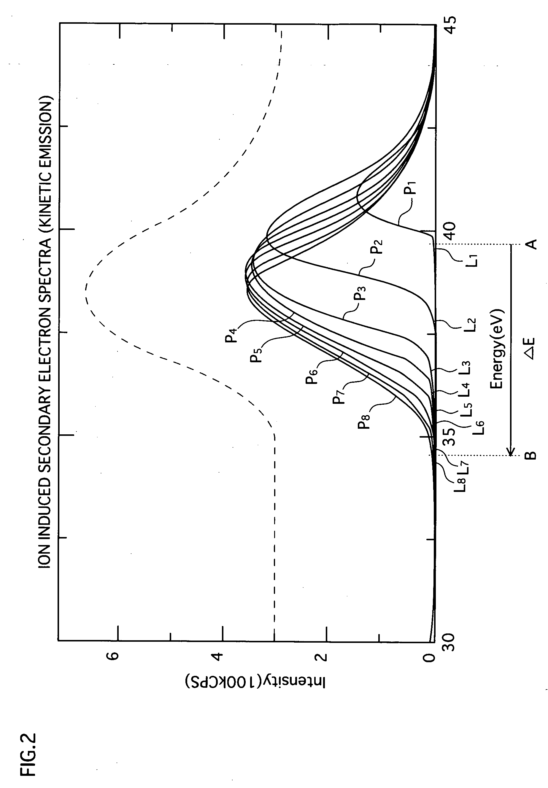
[0046] In the First Embodiment an MgO film formed on an Si substrate is used as a sample.
[0047] (Insulating Film Evaluating Device)
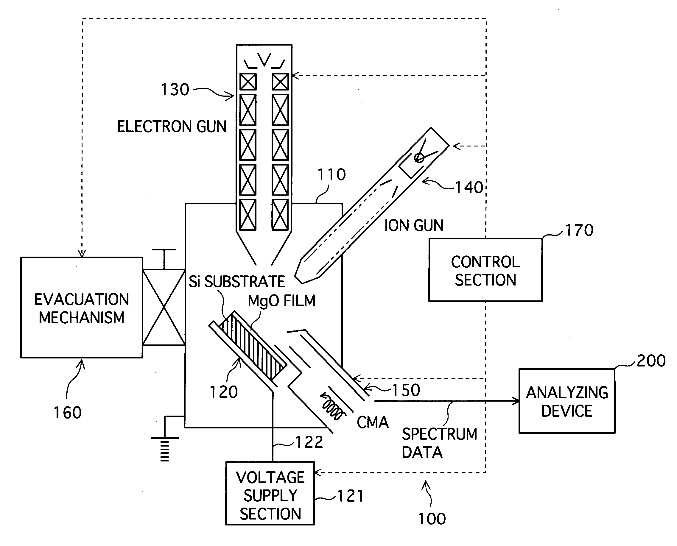
[0048]FIG. 1 is a schematic diagram showing a structure of an insulating film evaluating device of an embodiment of the present embodiment.
[0049] This evaluating device is constructed from a spectra measuring device 100 for measuring secondary electron spectra from the sample and an analyzing device 200 that, upon analysis of the measured secondary electron spectra, finds information (evaluation values) for evaluating the properties of the sample.
[0050] The spectra measuring device 100 is constructed from: a vacuum vessel 110; a sample stand 120 for mounting the sample (front panel); a voltage applying section 121 for applying a negative voltage to the sample; an electron gun 130 for irradiating the sample with electrons; an ion gun 140 for generating inert gas ions and irradiating the sample; a electron spectrograph (CMA) 150 for measuring the energ...
second embodiment
[0126]FIG. 7 is a perspective view showing the structure of the present embodiment of an AC surface discharge type PDP. As shown in the figure, the PDP is constructed with a front panel 10 and a back panel 20. The front panel includes display electrodes 12a and 12b, a dielectric layer 14, and a protective layer 15, on a front glass substrate 11. The back panel 20 includes data electrodes 22, barrier ribs 23 disposed in a stripe pattern, and phosphor layers 24 composed of red, green and blue ultra-violet light excited phosphors disposed between the barrier ribs 23, on a back glass substrate 21. The front panel 10 and the back panel 20 are joined so as to oppose one another and leave the space between them, and a discharge gas is enclosed in a space between the panels. Discharge cells are formed in the display area at points where the display electrodes and data electrodes cross over.
[0127] Further, when the PDP is manufactured, the display electrodes 12a and 12b, the dielectric laye...
PUM
 Abstract
Description
Claims
Application Information